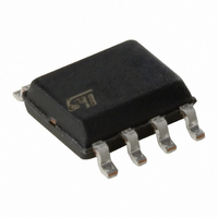
TS4890ID STMicroelectronics, TS4890ID Datasheet - Page 2

TS4890ID
Manufacturer Part Number
TS4890ID
Description
IC AMP AUDIO PWR 1W MONO 8SOIC
Manufacturer
STMicroelectronics
Type
Class ABr
Datasheet
1.TS4890ID.pdf
(32 pages)
Specifications of TS4890ID
Output Type
1-Channel (Mono)
Max Output Power X Channels @ Load
1W x 1 @ 8 Ohm
Voltage - Supply
2.5 V ~ 5.5 V
Features
Depop, Standby, Thermal Protection
Mounting Type
Surface Mount
Package / Case
8-SOIC (3.9mm Width)
Product
Class-A
Output Power
1 W
Thd Plus Noise
0.15 %
Operating Supply Voltage
3 V, 5 V
Supply Current
6 mA
Maximum Operating Temperature
+ 85 C
Mounting Style
SMD/SMT
Audio Load Resistance
8 Ohms
Input Offset Voltage
- 0.3 V to + 0.3 V
Input Signal Type
Single
Minimum Operating Temperature
- 40 C
Output Signal Type
Differential
Supply Type
Single
Supply Voltage (max)
5.5 V
Supply Voltage (min)
2.2 V
Operational Class
Class-A
Audio Amplifier Output Configuration
1-Channel Mono
Output Power (typ)
1x1@8OhmW
Audio Amplifier Function
Speaker
Total Harmonic Distortion
0.15@8Ohm@250mW%
Single Supply Voltage (typ)
3/5V
Dual Supply Voltage (typ)
Not RequiredV
Supply Current (max)
8@5VmA
Power Supply Requirement
Single
Unity Gain Bandwidth Product (typ)
2MHz
Rail/rail I/o Type
Rail to Rail Output
Power Supply Rejection Ratio
77dB
Single Supply Voltage (min)
2.2V
Single Supply Voltage (max)
5.5V
Dual Supply Voltage (min)
Not RequiredV
Dual Supply Voltage (max)
Not RequiredV
Operating Temp Range
-40C to 85C
Operating Temperature Classification
Industrial
Mounting
Surface Mount
Pin Count
8
Package Type
SO
Lead Free Status / RoHS Status
Contains lead / RoHS non-compliant
Other names
497-2292-5
Available stocks
Company
Part Number
Manufacturer
Quantity
Price
Part Number:
TS4890IDT
Manufacturer:
ST
Quantity:
20 000
TS4890
ABSOLUTE MAXIMUM RATINGS
1. All voltages values are measured with respect to the ground pin.
2. The magnitude of input signal must never exceed V
3. Device is protected in case of over temperature by a thermal shutdown active @ 150°C.
4. Exceeding the power derating curves during a long period may involve abnormal working of the device.
OPERATING CONDITIONS
1. This thermal resistance can be reduced with a suitable PCB layout (see Power Derating Curves Fig. 24)
2. When mounted on a 4 layers PCB
2/32
Symbol
Symbol
V
T
ESD
ESD
V
R
R
V
V
T
Pd
R
oper
STB
V
T
ICM
thja
thja
CC
stg
CC
L
i
j
Supply voltage
Input Voltage
Operating Free Air Temperature Range
Storage Temperature
Maximum Junction Temperature
Thermal Resistance Junction to Ambient
Power Dissipation
Human Body Model
Machine Model
Latch-up Immunity
Lead Temperature (soldering, 10sec)
Supply Voltage
Common Mode Input Voltage Range
Standby Voltage Input :
Load Resistor
Thermal Resistance Junction to Ambient
SO8
MiniSO8
DFN8
Device ON
Device OFF
SO8
MiniSO8
DFN8
2)
2)
1)
4)
Parameter
Parameter
CC
+ 0.3V / G
3)
1)
ND
- 0.3V
See Power Derating Curves
G
1.5
G
ND
ND
-65 to +150
G
-40 to + 85
2.2 to 5.5
ND
Class A
Fig. 24
+ 1V to V
V
Value
Value
4 - 32
V
150
175
215
200
260
150
190
STB
70
41
6
to V
2
STB
CC
V
0.5
CC
CC
°C/W
°C/W
Unit
Unit
kV
°C
°C
°C
°C
W
V
V
V
V
V
V


