TDA7256 STMicroelectronics, TDA7256 Datasheet
TDA7256
Specifications of TDA7256
Available stocks


Related parts for TDA7256


TDA7256 Summary of contents
Page 1
... Very inductive load - Overrating temperature - Open ground DESCRIPTION The TDA7256 is a class AB fully protected bridge power amplifier, designed for car radio applica- BLOCK DIAGRAM October 1998 This is advanced information on a new product now in development or undergoing evaluation. Details are subject to change without notice. ...
Page 2
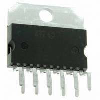
... TDA7256 PIN CONNECTION (Top view) ABSOLUTE MAXIMUM RATINGS Symbol V Operating Supply Voltage Supply Voltage S V Peak Supply Voltage (for 50ms Output Peak Current (non repetiitive t = 0.1ms Output Peak Current Repetitive f > 10Hz o P Power Dissipation (Tcase = 85 C) tot T T Storage and Junction Temperature Range ...
Page 3
... Figure 1: Test and Application Circuit = 14.4V 1KHz amb Test Condition Min 1KHz 100mV 10 3 0.1W to 13W 10K , B = 22Hz to 22KHz 10K , V = 1Vrms 300Hz V = 1Vrms, ref f = 100Hz to 10KHz Pin 1 2.4 Pin 1 Vref = 1Vrms TDA7256 = 25 C, unless otherwise Typ. Max. Unit 150 150 0. ...
Page 4
... TDA7256 Figure 2: P.C. and Layout of the fig.1 (1:1 scale) Figure 3: Drain Current vs. Supply Voltage 4/10 Figure 4: Output Power vs. Supply Voltage ...
Page 5
... Figure 5: Output Power vs. Supply Voltage Figure 7: Distortion vs. Output Power Figure 9: Distortion vs. Output Power Figure 6: Output Power vs. Supply Voltage Figure 8: Distortion vs. Output Power Figure 10: Distortion vs. Frequency TDA7256 5/10 ...
Page 6
... TDA7256 Figure 11: Distortion vs. Frequency Figure 13: CMRR vs. Frequency Figure 15: Power Dissipation & Efficiency vs. Output Power 6/10 Figure 12: SVR vs. Frequency Figure 14: Power Dissipation & Efficiency vs. Output Power Figure 16: Power Dissipation & Efficiency vs. Output Power ...
Page 7
... The mute circuit is also activated during turn- on/turn-off operations when the voltage at stand- by pin is lower than about 2 volt Figure 18: Soft Muting TURN-ON The TDA7256 is fully popless at turn-on thanks to a delay circuit which keeps the output low during the capacitors charge transient. The delay-time is given by the following formula: T ...
Page 8
... TDA7256 Figure 19: Silent Transients Through the Mute and Stand-by pins. 8/10 ...
Page 9
... S 1.9 2.6 0.075 S1 1.9 2.6 0.075 Dia1 3.65 3.85 0.144 OUTLINE AND MAX. MECHANICAL DATA 0.197 0.104 0.063 0.022 0.037 0.077 0.679 0.795 0.886 0.886 0.713 0.699 0.429 0.114 0.191 0.214 0.102 Multiwatt11 V 0.102 0.152 TDA7256 9/10 ...
Page 10
... TDA7256 Information furnished is believed to be accurate and reliable. However, SGS-THOMSON Microelectronics assumes no responsibility for the consequences of use of such information nor for any infringement of patents or other rights of third parties which may result from its use. No license is granted by implication or otherwise under any patent or patent rights of SGS-THOMSON Microelectronics. Specifications men- tioned in this publication are subject to change without notice ...