STA540 STMicroelectronics, STA540 Datasheet - Page 20
STA540
Manufacturer Part Number
STA540
Description
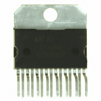
IC AMP AUD DUAL/QUAD MULTIWATT15
Manufacturer
STMicroelectronics
Type
Class ABr
Datasheet
1.STA540.pdf
(23 pages)
Specifications of STA540
Output Type
2-Channel (Stereo) or 4-Channel (Quad)
Max Output Power X Channels @ Load
38W x 2 @ 4 Ohm; 16W x 4 @ 4 Ohm
Voltage - Supply
8 V ~ 22 V
Features
Short-Circuit and Thermal Protection, Standby
Mounting Type
Through Hole
Package / Case
Multiwatt-15 (Vertical, Bent and Staggered Leads)
Amplifier Class
AB
No. Of Channels
4
Output Power
24W
Supply Voltage Range
8V To 22V
Thd + N
0.02% @ 4W, 4ohm, VS=14.4V
Load Impedance
8ohm
Operating Temperature Range
-40°C To +150°C
Rohs Compliant
Yes
Lead Free Status / RoHS Status
Lead free / RoHS Compliant
Other names
497-8880-5
Available stocks
Company
Part Number
Manufacturer
Quantity
Price
Company:

Part Number:
STA540
Manufacturer:
FOXCONN
Quantity:
2 300
Part Number:
STA540
Manufacturer:
ST
Quantity:
20 000
Company:
Part Number:
STA540SA
Manufacturer:
ST
Quantity:
12 000
Part Number:
STA540SA
Manufacturer:
ST
Quantity:
20 000
Part Number:
STA540SAN
Manufacturer:
ST
Quantity:
20 000


Practical information
6.9
6.10
20/23
PCB ground layout
The device has two distinct ground pins, P-GND (power ground) and S-GND (signal ground)
which are disconnected from each other at chip level. For superior performance the pins
P-GND and S-GND must be connected together on the PCB by low-resistance tracks.
For the PCB-ground configuration, a star-like arrangement, where the center is represented
by the supply-filtering electrolytic capacitor ground, is recommended. In an arrangement
such as this, at least two separate paths must be provided, one for P-GND and one for
S-GND.
The correct ground assignments are as follows:
"
"
Mute function
If the mute function is desired, it can be implemented on pin 6, SVR, as shown in
Figure 29. Optional mute function circuit
Using a different value for R1 than the suggested 3.3 kΩ, results in two different situations:
"
"
V
mute off: V
mute on: V
S
= 10 to 16 V,
on S-GND:
–
–
–
on P-GND:
–
R1 > 3.3 kΩ:
–
–
R1 < 3.3 kΩ:
–
–
standby capacitor (pin 7, or any other standby driving networks),
SVR capacitor (pin 6), to be placed as close as possible to the device,
input signal ground (from active/passive signal processor stages)
power supply filtering capacitors for pins 3 and 13. The negative terminal of the
electrolytic capacitor(s) must be directly tied to the battery negative line and this
should represent the starting point for all the ground paths.
pop noise improvement,
lower mute attenuation;
pop noise degradation,
higher mute attenuation.
SVR
SVR
≥ 0.6 to 0.8 V,
≥ 0.2 V
PLAY
0
MUTE
5V
R2 10K
IN BRIDGE
ST-BY
IN R
IN L
R1 3.3K
10K
0.22µF
0.22µF
0.47µF
470µF
10µF
4
5
12
11
6
8
7
9
13
DIAGNOSTICS
3
10
100nF
15
14
1
2
2200µF
2200µF
D06AU1632
1000µF
BRIDGE
OUT R
OUT L
OUT
V S
Figure
STA540
29.
Related parts for STA540
Image
Part Number
Description
Manufacturer
Datasheet
Request
R

Part Number:
Description:
STMicroelectronics [RIPPLE-CARRY BINARY COUNTER/DIVIDERS]
Manufacturer:
STMicroelectronics
Datasheet:
Part Number:
Description:
STMicroelectronics [LIQUID-CRYSTAL DISPLAY DRIVERS]
Manufacturer:
STMicroelectronics
Datasheet:

Part Number:
Description:
BOARD EVAL FOR MEMS SENSORS
Manufacturer:
STMicroelectronics
Datasheet:
Part Number:
Description:
NPN TRANSISTOR POWER MODULE
Manufacturer:
STMicroelectronics
Datasheet:
Part Number:
Description:
TURBOSWITCH ULTRA-FAST HIGH VOLTAGE DIODE
Manufacturer:
STMicroelectronics
Datasheet:
Part Number:
Description:
Manufacturer:
STMicroelectronics
Datasheet:
Part Number:
Description:
DIODE / SCR MODULE
Manufacturer:
STMicroelectronics
Datasheet:
Part Number:
Description:
DIODE / SCR MODULE
Manufacturer:
STMicroelectronics
Datasheet:
Part Number:
Description:
Search -----> STE16N100
Manufacturer:
STMicroelectronics
Datasheet:
Part Number:
Description:
Search ---> STE53NA50
Manufacturer:
STMicroelectronics
Datasheet:
Part Number:
Description:
NPN Transistor Power Module
Manufacturer:
STMicroelectronics
Datasheet:
Part Number:
Description:
DIODE / SCR MODULE
Manufacturer:
STMicroelectronics
Datasheet: