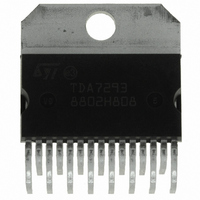
TDA7293HS STMicroelectronics, TDA7293HS Datasheet - Page 11

TDA7293HS
Manufacturer Part Number
TDA7293HS
Description
IC AMP AUDIO 100W AB MULTIWATT15
Manufacturer
STMicroelectronics
Type
Class ABr
Datasheet
1.TDA7293V.pdf
(21 pages)
Specifications of TDA7293HS
Output Type
1-Channel (Mono)
Max Output Power X Channels @ Load
100W x 1 @ 4 Ohm
Voltage - Supply
±12 V ~ 50 V
Features
Depop, Differential Inputs, Mute, Short-Circuit and Thermal Protection, Standby
Mounting Type
Through Hole
Package / Case
Multiwatt-15 (Horizontal, Bent and Staggered Leads)
Amplifier Class
AB
No. Of Channels
1
Output Power
100W
Supply Voltage Range
± 12V To ± 15V
Thd + N
0.005% @ 5W, 8ohm, VS=± 40V
Load Impedance
8ohm
Operating Temperature Range
0°C To +70°C
Rohs Compliant
Yes
Lead Free Status / RoHS Status
Lead free / RoHS Compliant
Other names
497-8865-5
TDA7293HS
TDA7293HS
TDA7293
4.2
4.3
High efficiency
Constraints of implementing high power solutions are the power dissipation and the size of
the power supply. These are both due to the low efficiency of conventional AB class
amplifier approaches.
The circuit below in
and car-radio applications. The TDA7293 is a monolithic MOS power amplifier which can be
operated with a 100-V supply (120 V with no signal applied) while delivering output currents
up to ±6.5 A. This allows the use of this device as a very high-power amplifier (up to 180 W
peak power with THD = 10% and R
hardly manageable in the above power range.
The typical junction-to-case thermal resistance of the TDA7293 is 1 °C/W (max = 1.5 °C/W).
In worst case conditions, to avoid the chip temperature exceeding 150 °C the thermal
resistance of the heatsink must be 0.038 °C/W (at a maximum ambient temperature of
50 °C).
As the above value is pratically unreachable, a high efficiency system is needed in those
cases where the continuous average output power is higher than 50 to 60 W.
The TDA7293 was designed to work also in a higher efficiency way. For this reason there
are four power supply pins: two intended for the signal part and two for the power part. T1
and T2 are two power transistors that only operate when the output power reaches a certain
threshold (for example, 20 W).
If the output power increases, these transistors are switched on during the portion of the
signal where more output voltage swing is needed, thus "bootstrapping" the power supply
pins (13 and 15). The current generators formed by T4, T7, zener diodes Z1, Z2 and
resistors R7, R8 define the minimum drop across the power MOS transistors of the
TDA7293. L1, L2, L3 and the snubbers C9, R1 and C10, R2 stabilize the loops formed by
the "bootstrap" circuits and the output stage of the TDA7293.
By considering again a maximum average output power (music signal) of 20 W, in case of
the high efficiency application, the thermal resistance value needed from the heatsink is
2.2 °C/W (with V
T1 and T2) can be placed on a 1.5 °C/W heatsink, with the power darlingtons electrically
insulated from the heatsink.
Since the total power dissipation is less than that of a usual class AB amplifier, additional
cost savings can be obtained while optimizing the power supply, even with a large heatsink.
Bridge application
Another application suggestion is the bridge configuration, where two TDA7293 are used.
In this application, the value of the load must not be lower than 8 Ω for dissipation and
current capability reasons.
A suitable field of application includes hi-fi/TV subwoofer realizations. The main advantages
offered by this solution are:
With R
R
L
= 16 Ω and V
High power performance with limited supply voltage level.
Considerably higher output power even with high load values, such as 16 Ω.
L
= 8 Ω and V
S
S
= ±50 V and R
= ±40 V, the maximum Pout is 200 W.
Figure 8
S
= ±25 V, the maximum output power obtainable is 150 W, whilst with
is a high efficiency amplifier which can be adopted for both hi-fi
Doc ID 6744 Rev 8
L
= 8 Ω). All components (TDA7293 and power transistors
L
= 4 Ω); the only drawback is the power dissipation,
Applications information
11/21


