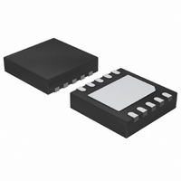
NCP4894MNR2G ON Semiconductor, NCP4894MNR2G Datasheet - Page 13

NCP4894MNR2G
Manufacturer Part Number
NCP4894MNR2G
Description
IC AMP AUDIO PWR 1W DIFF 10-DFN
Manufacturer
ON Semiconductor
Type
Class ABr
Datasheet
1.NCP4894DMR2G.pdf
(19 pages)
Specifications of NCP4894MNR2G
Output Type
1-Channel (Mono)
Max Output Power X Channels @ Load
1.8W x 1 @ 8 Ohm
Voltage - Supply
2.2 V ~ 5.5 V
Features
Depop, Differential Inputs, Short-Circuit and Thermal Protection, Shutdown
Mounting Type
Surface Mount
Package / Case
10-VFDFN Exposed Pad
Operational Class
Class-AB
Audio Amplifier Output Configuration
1-Channel Mono
Output Power (typ)
1.08x1@8OhmW
Audio Amplifier Function
Speaker
Total Harmonic Distortion
0.006@8Ohm@1000mW%
Single Supply Voltage (typ)
3/5V
Dual Supply Voltage (typ)
Not RequiredV
Power Supply Requirement
Single
Rail/rail I/o Type
No
Power Supply Rejection Ratio
85dB
Single Supply Voltage (min)
2.2V
Single Supply Voltage (max)
5.5V
Dual Supply Voltage (min)
Not RequiredV
Dual Supply Voltage (max)
Not RequiredV
Operating Temp Range
-40C to 85C
Operating Temperature Classification
Industrial
Mounting
Surface Mount
Pin Count
10
Lead Free Status / RoHS Status
Lead free / RoHS Compliant
Other names
NCP4894MNR2G
NCP4894MNR2GOSTR
NCP4894MNR2GOSTR
Available stocks
Company
Part Number
Manufacturer
Quantity
Price
Company:
Part Number:
NCP4894MNR2G
Manufacturer:
ON Semiconductor
Quantity:
500
Gain−Setting Resistor Selection (R
NCP4894 should be used in low gain configurations.
values and maximizes the signal to noise ratio, and the
amplifier can still be used without running into the
bandwidth limitations.
recommended to optimize overall system performance.
applications, and doesn’t require the use of a very large
capacitor C
Input Capacitor Selection (C
the amplifier input terminal. This capacitor creates a
high−pass filter with Rin, the cut−off frequency is given by
fc
J2
R
In order to optimize device and system performance, the
The low gain configuration minimizes THD + noise
A closed loop gain in the range from 2 to 5 is
An input resistor (R
The input coupling capacitor blocks the DC voltage at
+
in
2 * P * R in * C in
and R
in
f
1
100 kW
set the closed−loop gain of both amplifiers.
.
1 mF
C2
1 mF
C1
R3
.
J1
in
) value of 22 kW is realistic in most
J10
J5
20 kW
in
20 kW
R1
GND
VP
VP
)
R2
J4
C3
in
Figure 31. Demonstration Board Schematic
and R
1 mF
f
)
BYPASS
SD SELECT
SD MODE
INP
INM
http://onsemi.com
NCP4894
BYPASS
BYPASS
13
VP
in low frequencies without severe attenuation. However a
large input coupling capacitor requires more time to reach
its quiescent DC voltage (VP/2) and can increase the
turn−on pops.
performs well in many applications (With R
Bypass Capacitor Selection (Cby)
and determines how fast the NCP4894 turns on.
turn−on pop. A 1.0 mF bypass capacitor value
(C
shutdown transitions. The amplifier is still functional with
a 0.1 mF capacitor value but is more susceptible to “pop and
click” noises.
VMC
BRIDGE
20 kW
20 kW
VP
The size of the capacitor must be large enough to couple
An input capacitor value between 0.1 m and 0.39 mF
The bypass capacitor Cby provides half−supply filtering
This capacitor is a critical component to minimize the
Thus, a 1.0 mF bypassing capacitor is recommended.
VP
in
R5
R4
VM
= < 0.39 mF) should produce clickless and popless
C4
1 mF
SHUTDOWN
CONTROL
+
−
−
+
OUTA
OUTB
J3
in
= 22 kW).
RL
8W


