NCP4894MNR2G ON Semiconductor, NCP4894MNR2G Datasheet - Page 4
NCP4894MNR2G
Manufacturer Part Number
NCP4894MNR2G
Description
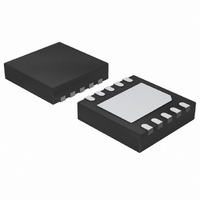
IC AMP AUDIO PWR 1W DIFF 10-DFN
Manufacturer
ON Semiconductor
Type
Class ABr
Datasheet
1.NCP4894DMR2G.pdf
(19 pages)
Specifications of NCP4894MNR2G
Output Type
1-Channel (Mono)
Max Output Power X Channels @ Load
1.8W x 1 @ 8 Ohm
Voltage - Supply
2.2 V ~ 5.5 V
Features
Depop, Differential Inputs, Short-Circuit and Thermal Protection, Shutdown
Mounting Type
Surface Mount
Package / Case
10-VFDFN Exposed Pad
Operational Class
Class-AB
Audio Amplifier Output Configuration
1-Channel Mono
Output Power (typ)
1.08x1@8OhmW
Audio Amplifier Function
Speaker
Total Harmonic Distortion
0.006@8Ohm@1000mW%
Single Supply Voltage (typ)
3/5V
Dual Supply Voltage (typ)
Not RequiredV
Power Supply Requirement
Single
Rail/rail I/o Type
No
Power Supply Rejection Ratio
85dB
Single Supply Voltage (min)
2.2V
Single Supply Voltage (max)
5.5V
Dual Supply Voltage (min)
Not RequiredV
Dual Supply Voltage (max)
Not RequiredV
Operating Temp Range
-40C to 85C
Operating Temperature Classification
Industrial
Mounting
Surface Mount
Pin Count
10
Lead Free Status / RoHS Status
Lead free / RoHS Compliant
Other names
NCP4894MNR2G
NCP4894MNR2GOSTR
NCP4894MNR2GOSTR
Available stocks
Company
Part Number
Manufacturer
Quantity
Price
Company:

Part Number:
NCP4894MNR2G
Manufacturer:
ON Semiconductor
Quantity:
500


1. The SD SELECT pin must be toggled to the same state as the SD MODE pin to force the device in shutdown mode.
PIN DESCRIPTION
9−Pin Flip−Chip
INM SD SELECT OUTA
INP
VP
B1
A1
C1
C1
C2
C3
A1
A2
A3
B1
B2
B3
9−Pin Flip−Chip
SD MODE
BYPASS
(Top View)
A2
C2
B2
Micro−10/DFN10
OUTB
B3
VM
A3
C3
10
4
5
6
9
3
7
2
1
SD SELECT
SD MODE
Type
BYPASS
O
O
I
I
I
I
I
I
I
INM
INP
SD SELECT
SD MODE
BYPASS
Symbol
OUTB
OUTA
PIN CONNECTIONS
1
2
3
4
5
INM
INP
VM
http://onsemi.com
VP
NCP4894
Micro−10
(Top View)
4
Positive Differential Input
Bypass Capacitor Pin which Provides the Common Mode Voltage
Negative BTL Output
Positive Analog Supply of the Cell
Shutdown High or Low Selectivity (Note 1)
Ground
Negative Differential Input
(Note 1)
Positive BTL Output
10
9
8
7
6
OUTA
VP
NC
VM
OUTB
SD SELECT
SD MODE
BYPASS
Description
INM
INP
1
2
3
4
5
(Top View)
DFN10
10
9
8
7
6
OUTA
VP
NC
VM
OUTB
Related parts for NCP4894MNR2G
Image
Part Number
Description
Manufacturer
Datasheet
Request
R

Part Number:
Description:
Differential Audio Power Amplifier
Manufacturer:
ON Semiconductor
Datasheet:

Part Number:
Description:
EVAL BOARD FOR NCP4894FC
Manufacturer:
ON Semiconductor
Datasheet:
Part Number:
Description:
ON Semiconductor [VOLTAGE REGULATOR]
Manufacturer:
ON Semiconductor
Datasheet:
Part Number:
Description:
357-036-542-201 CARDEDGE 36POS DL .156 BLK LOPRO
Manufacturer:
ON Semiconductor
Datasheet:
Part Number:
Description:
357-036-542-201 CARDEDGE 36POS DL .156 BLK LOPRO
Manufacturer:
ON Semiconductor
Datasheet:
Part Number:
Description:
357-036-542-201 CARDEDGE 36POS DL .156 BLK LOPRO
Manufacturer:
ON Semiconductor
Datasheet:
Part Number:
Description:
357-036-542-201 CARDEDGE 36POS DL .156 BLK LOPRO
Manufacturer:
ON Semiconductor
Datasheet:
Part Number:
Description:
357-036-542-201 CARDEDGE 36POS DL .156 BLK LOPRO
Manufacturer:
ON Semiconductor
Datasheet:
Part Number:
Description:
357-036-542-201 CARDEDGE 36POS DL .156 BLK LOPRO
Manufacturer:
ON Semiconductor
Datasheet:
Part Number:
Description:
357-036-542-201 CARDEDGE 36POS DL .156 BLK LOPRO
Manufacturer:
ON Semiconductor
Datasheet:
Part Number:
Description:
357-036-542-201 CARDEDGE 36POS DL .156 BLK LOPRO
Manufacturer:
ON Semiconductor
Datasheet:
Part Number:
Description:
357-036-542-201 CARDEDGE 36POS DL .156 BLK LOPRO
Manufacturer:
ON Semiconductor
Datasheet:
Part Number:
Description:
357-036-542-201 CARDEDGE 36POS DL .156 BLK LOPRO
Manufacturer:
ON Semiconductor
Datasheet:
Part Number:
Description:
Manufacturer:
ON Semiconductor
Datasheet: