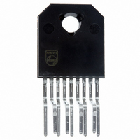
TFA9842J/N1,112 NXP Semiconductors, TFA9842J/N1,112 Datasheet - Page 7

TFA9842J/N1,112
Manufacturer Part Number
TFA9842J/N1,112
Description
IC AMP AUDIO PWR 15W STER 9SIL
Manufacturer
NXP Semiconductors
Type
Class ABr
Datasheet
1.TFA9842JN1112.pdf
(21 pages)
Specifications of TFA9842J/N1,112
Output Type
1-Channel (Mono) or 2-Channel (Stereo)
Package / Case
9-SIL (Bent and Staggered Leads)
Max Output Power X Channels @ Load
15W x 1 @ 8 Ohm; 7.5W x 2 @ 4 Ohm
Voltage - Supply
9 V ~ 26 V
Features
Depop, Mute, Short-Circuit and Thermal Protection, Standby
Mounting Type
Through Hole
Product
Class-AB
Output Power
7.5 W, 15 W
Available Set Gain
26 dB, 32 dB
Thd Plus Noise
0.1 %, 0.05 %
Operating Supply Voltage
17 V
Supply Current
60 mA
Maximum Power Dissipation
35 W
Maximum Operating Temperature
+ 85 C
Mounting Style
SMD/SMT
Audio Load Resistance
8 Ohms
Minimum Operating Temperature
- 40 C
Supply Voltage (max)
26 V
Supply Voltage (min)
9 V
Lead Free Status / RoHS Status
Lead free / RoHS Compliant
Other names
568-3453-5
935274136112
TFA9842J
935274136112
TFA9842J
Philips Semiconductors
9. Limiting values
Table 6:
In accordance with the Absolute Maximum Rating System (IEC 60134).
10. Thermal characteristics
Table 7:
11. Static characteristics
Table 8:
V
[1]
[2]
[3]
[4]
9397 750 12013
Preliminary data
Symbol
V
V
I
T
T
P
V
Symbol
R
R
Symbol
V
I
I
V
V
I
ORM
q
stb
MODE
CC
stg
amb
V
CC
I
tot
CC(sc)
CC
O
MODE
th(j-a)
th(j-c)
OUT
= 17 V; T
A minimum load for BTL of 16
With a load connected at the outputs the quiescent supply current will increase.
The DC output voltage with respect to ground is approximately 0.5V
V
OUT
= V
Limiting values
Thermal characteristics
Static characteristics
Parameter
supply voltage
input voltage
repetitive peak output current
storage temperature
ambient temperature
total power dissipation
supply voltage to guarantee short-circuit
protection
Parameter
thermal resistance from junction to ambient
thermal resistance from junction to case
Parameter
supply voltage
quiescent supply current
standby supply current
DC output voltage
differential output voltage offset BTL mode
mode selection input voltage
input current on pin MODE
amb
OUT1+
= 25 C; R
V
OUT2
L
= 8 ; V
is required at V
MODE
= V
Conditions
operating
R
V
on mode
mute mode
standby mode
0 < V
CC
MODE
CC
L
=
; V
> 22 V.
MODE
Rev. 01 — 26 April 2004
i
= 0
= 0 V; measured in test circuit
< V
Conditions
operating
no signal
non-operating
operating
CC
Conditions
in free air
both channels driven
CC
3.5
.
2-channel audio amplifier (2 x SE or 1 x BTL)
[1]
[2]
[3]
[4]
Min
9
-
-
-
-
V
4.5
0
-
CC
2.0
Figure
Min
-
-
-
Typ
17
60
-
9
-
-
-
-
-
0.3
0.3
0.3
55
40
© Koninklijke Philips Electronics N.V. 2004. All rights reserved.
13; unless otherwise specified.
Max
+26
+28
V
3
+150
+85
35
24
Value
40
2.0
Max
26
100
10
-
200
V
V
0.8
20
TFA9842J
CC
CC
CC
+ 0.3
3.5
Unit
V
V
V
A
W
V
Unit
K/W
K/W
Unit
V
mA
V
mV
V
V
V
C
C
A
A
7 of 21


