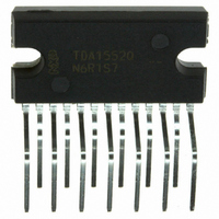
TDA1552Q/N4,112 NXP Semiconductors, TDA1552Q/N4,112 Datasheet - Page 4

TDA1552Q/N4,112
Manufacturer Part Number
TDA1552Q/N4,112
Description
IC AMP AUDIO PWR 22W QUAD 13SIL
Manufacturer
NXP Semiconductors
Type
Class Br
Datasheet
1.TDA1552QN4112.pdf
(10 pages)
Specifications of TDA1552Q/N4,112
Package / Case
13-SIL (Bent and Staggered Leads)
Output Type
4-Channel (Quad)
Max Output Power X Channels @ Load
22W x 2 @ 4 Ohm
Voltage - Supply
6 V ~ 18 V
Features
Depop, Mute, Short-Circuit and Thermal Protection, Standby
Mounting Type
Through Hole
Operating Supply Voltage
18 V
Supply Current
80 mA
Maximum Operating Temperature
150 C
Mounting Style
SMD/SMT
Minimum Operating Temperature
- 55 C
Operational Class
Class-B
Audio Amplifier Output Configuration
2-Channel Stereo
Output Power (typ)
22x2W
Audio Amplifier Function
Speaker
Total Harmonic Distortion
0.1%
Single Supply Voltage (typ)
14.4V
Dual Supply Voltage (typ)
Not RequiredV
Power Supply Requirement
Single
Power Dissipation
60W
Rail/rail I/o Type
No
Single Supply Voltage (min)
6V
Single Supply Voltage (max)
18V
Dual Supply Voltage (min)
Not RequiredV
Dual Supply Voltage (max)
Not RequiredV
Mounting
Through Hole
Pin Count
13
Package Type
DBS13P
Lead Free Status / RoHS Status
Lead free / RoHS Compliant
Lead Free Status / RoHS Status
Lead free / RoHS Compliant, Lead free / RoHS Compliant
Other names
568-3506-5
935054880112
TDA1552QU
935054880112
TDA1552QU
Philips Semiconductors
PINNING
FUNCTIONAL DESCRIPTION
The TDA1552Q contains two identical amplifiers with differential input stages and can be used for bridge applications.
The gain of each amplifier is fixed at 26 dB. A special feature of this device is:
Mute/stand-by switch
RATINGS
Limiting values in accordance with the Absolute Maximum System (IEC 134)
July 1994
1
2
3
4
5
6
7
Supply voltage
Non-repetitive peak output current
Repetitive peak output current
Storage temperature range
Junction temperature
AC and DC short-circuit-safe voltage
Energy handling capability at outputs
Reverse polarity
Total power dissipation
low stand-by current (< 100 A)
low mute/stand-by switching current (low cost supply switch)
mute facility.
2 x 22 W BTL stereo car radio power
amplifier
operating
non-operating
load dump protected
IP1
GND
V
OUT1A
GND1
OUT1B
OUT2A
P1
PARAMETER
input 1
ground (signal)
positive supply voltage 1
output 1A
power ground 1 (substrate)
output 1B
output 2A
during 50 ms;
t
V
see Fig.2
r
P
CONDITIONS
= 0 V
2.5 ms
4
10
11
12
13
8
9
GND2
OUT2B
V
M/SS
n.c.
IP2
P2
V
V
V
I
I
T
T
V
V
P
SYMBOL
OSM
ORM
stg
j
P
P
P
PSC
PR
tot
power ground 2 (substrate)
output 2B
positive supply voltage 2
mute/stand-by switch
not connected
input 2
55
MIN.
18
30
45
6
4
150
18
200
6
60
150
MAX.
Product specification
TDA1552Q
V
V
V
A
A
V
mJ
V
W
C
C
UNIT


