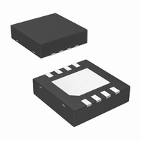
LM4810LD/NOPB National Semiconductor, LM4810LD/NOPB Datasheet - Page 11

LM4810LD/NOPB
Manufacturer Part Number
LM4810LD/NOPB
Description
IC AMP AUDIO PWR .105W STER 8LLP
Manufacturer
National Semiconductor
Series
Boomer®r
Type
Class ABr
Datasheet
1.LM4810MMNOPB.pdf
(18 pages)
Specifications of LM4810LD/NOPB
Output Type
Headphones, 2-Channel (Stereo)
Max Output Power X Channels @ Load
105mW x 2 @ 16 Ohm
Voltage - Supply
2 V ~ 5.5 V
Features
Depop, Shutdown, Thermal Protection
Mounting Type
Surface Mount
Package / Case
8-LLP
Lead Free Status / RoHS Status
Lead free / RoHS Compliant
Other names
LM4810LD
LM4810LDTR
LM4810LDTR
Available stocks
Company
Part Number
Manufacturer
Quantity
Price
Company:
Part Number:
LM4810LD/NOPB
Manufacturer:
TI/NSC
Quantity:
18 720
Typical Performance Characteristics
Application Information
MICRO-POWER SHUTDOWN
The voltage applied to the SHUTDOWN pin controls the
LM4810’s shutdown function. Activate micro-power shut-
down by applying a logic high voltage to the SHUTDOWN
pin. The logic threshold is typically V
LM4810’s micro-power shutdown feature turns off the ampli-
fier’s bias circuitry, reducing the supply current. The low
0.4µA typical shutdown current is achieved by applying a
voltage that is as near as V
DOWN pin. A voltage that is less than V
shutdown current.
There are a few ways to control the micro-power shutdown.
These include using a single-pole, single-throw switch, a
microprocessor, or a microcontroller. When using a switch,
connect an external 100kΩ pull-up resistor between the
SHUTDOWN pin and V
SHUTDOWN pin and GND. Select normal amplifier opera-
tion by closing the switch. Opening the switch connects the
SHUTDOWN pin to V
ing micro-power shutdown. The switch and resistor guaran-
tee that the SHUTDOWN pin will not float. This prevents
unwanted state changes. In a system with a microprocessor
or a microcontroller, use a digital output to apply the control
voltage to the SHUTDOWN pin. Driving the SHUTDOWN pin
with active circuitry eliminates the pull-up resistor.
EXPOSED-DAP PACKAGE PCB MOUNTING
CONSIDERATION
The LM4810’s exposed-Dap (die attach paddle) package
(LD) provides a low thermal resistance between the die and
the PCB to which the part is mounted and soldered. This
allows rapid heat transfer from the die to the surrounding
PCB copper traces, ground plane, and surrounding air.
The LD package should have its DAP soldered to a copper
pad on the PCB. The DAP’s PCB copper pad may be con-
nected to a large plane of continuous unbroken copper. This
plane forms a thermal mass, heat sink, and radiation area.
However, since the LM4810 is designed for headphone ap-
plications, connecting a copper plane to the DAP’s PCB
Frequency Response
DD
DD
through the pull-up resistor, activat-
Open Loop
. Connect the switch between the
DD
as possible to the SHUT-
DD
DD
/2. When active, the
may increase the
20008938
11
(Continued)
copper pad is not required. The LM4810’s Power Dissipation
vs Output Power Curve in the Typical Performance Char-
acteristics shows that the maximum power dissipated is just
45mW per amplifier with a 5V power supply and a 32Ω load.
Further detailed and specific information concerning PCB
layout, fabrication, and mounting an LD (LLP) package is
available from National Semiconductor’s Package Engineer-
ing Group under application note AN1187.
POWER DISSIPATION
Power dissipation is a major concern when using any power
amplifier and must be thoroughly understood to ensure a
successful design. Equation 1 states the maximum power
dissipation point for a single-ended amplifier operating at a
given supply voltage and driving a specified output load.
Since the LM4810 has two operational amplifiers in one
package, the maximum internal power dissipation point is
twice that of the number which results from Equation 1. Even
with the large internal power dissipation, the LM4810 does
not require heat sinking over a large range of ambient tem-
perature. From Equation 1, assuming a 5V power supply and
a 32Ω load, the maximum power dissipation point is 40mW
per amplifier. Thus the maximum package dissipation point
is 80mW. The maximum power dissipation point obtained
must not be greater than the power dissipation that results
from Equation 2:
For package MUA08A, θ
the LM4810. Depending on the ambient temperature, T
the system surroundings, Equation 2 can be used to find the
maximum internal power dissipation supported by the IC
packaging. If the result of Equation 1 is greater than that of
Equation 2, then either the supply voltage must be de-
P
P
DMAX
DMAX
Supply Current vs
Supply Voltage
= (T
= (V
JA
JMAX
DD
= 210˚C/W. T
)
2
− T
/ (2π
A
) / θ
2
R
L
JA
)
JMAX
20008944
= 150˚C for
www.national.com
A
, of
(1)
(2)


