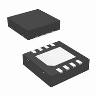
LM4810LD/NOPB National Semiconductor, LM4810LD/NOPB Datasheet - Page 13

LM4810LD/NOPB
Manufacturer Part Number
LM4810LD/NOPB
Description
IC AMP AUDIO PWR .105W STER 8LLP
Manufacturer
National Semiconductor
Series
Boomer®r
Type
Class ABr
Datasheet
1.LM4810MMNOPB.pdf
(18 pages)
Specifications of LM4810LD/NOPB
Output Type
Headphones, 2-Channel (Stereo)
Max Output Power X Channels @ Load
105mW x 2 @ 16 Ohm
Voltage - Supply
2 V ~ 5.5 V
Features
Depop, Shutdown, Thermal Protection
Mounting Type
Surface Mount
Package / Case
8-LLP
Lead Free Status / RoHS Status
Lead free / RoHS Compliant
Other names
LM4810LD
LM4810LDTR
LM4810LDTR
Available stocks
Company
Part Number
Manufacturer
Quantity
Price
Company:
Part Number:
LM4810LD/NOPB
Manufacturer:
TI/NSC
Quantity:
18 720
Application Information
the magnitude of “clicks and pops”. Increasing the value of
C
presents a tradeoff: as the size of C
time increases. There is a linear relationship between the
size of C
turn-on times for various values of C
In order eliminate “clicks and pops”, all capacitors must be
discharged before turn-on. Rapidly switching V
allow the capacitors to fully discharge, which may cause
“clicks and pops”. In a single-ended configuration, the output
is coupled to the load by C
high value. C
Depending on the size of C
can be relatively large. To reduce transients in single-ended
mode, an external 1kΩ–5kΩ resistor can be placed in par-
allel with the internal 20kΩ resistor. The tradeoff for using
this resistor is increased quiescent current.
AUDIO POWER AMPLIFIER DESIGN
Design a Dual 70mW/32Ω Audio Amplifier
The design begins by specifying the minimum supply voltage
necessary to obtain the specified output power. One way to
find the minimum supply voltage is to use the Output Power
vs Supply Voltage curve in the Typical Performance Char-
acteristics section. Another way, using Equation (5), is to
calculate the peak output voltage necessary to achieve the
desired output power for a given load impedance. To ac-
count for the amplifier’s dropout voltage, two additional volt-
ages, based on the Dropout Voltage vs Supply Voltage in the
Typical Performance Characteristics curves, must be
added to the result obtained by Equation (5). For a
single-ended application, the result is Equation (6).
Given:
Power Output
Load Impedance
Input Level
Input Impedance
Bandwidth
B
reduces the magnitude of turn-on pops. However, this
B
and the turn-on time. Here are some typical
O
0.22µF
0.33µF
0.47µF
0.68µF
0.1µF
1.0µF
2.2µF
3.3µF
4.7µF
10µF
discharges through internal 20kΩ resistors.
C
B
O
O
. This capacitor usually has a
, the discharge time constant
920ms
1.8sec
2.8sec
3.4sec
7.7sec
100 Hz–20 kHz
B
B
increases, the turn-on
:
170ms
270ms
370ms
490ms
80ms
T
ON
(Continued)
1 Vrms (max)
DD
±
may not
70 mW
0.50dB
20kΩ
32Ω
(5)
13
The Output Power vs Supply Voltage graph for a 32Ω load
indicates a minimum supply voltage of 4.8V. This is easily
met by the commonly used 5V supply voltage. The additional
voltage creates the benefit of headroom, allowing the
LM4810 to produce peak output power in excess of 70mW
without clipping or other audible distortion. The choice of
supply voltage must also not create a situation that violates
maximum power dissipation as explained above in the
Power Dissipation section. Remember that the maximum
power dissipation point from Equation (1) must be multiplied
by two since there are two independent amplifiers inside the
package. Once the power dissipation equations have been
addressed, the required gain can be determined from Equa-
tion (7).
Thus, a minimum gain of 1.497 allows the LM4810 to reach
full output swing and maintain low noise and THD+N perfro-
mance. For this example, let A
The amplifiers overall gain is set using the input (R
feedback (R
set at 20kΩ, the feedback resistor is found using Equation
(8).
The value of R
The last step in this design is setting the amplifier’s −3db
frequency bandwidth. To achieve the desired
band magnitude variation limit, the low frequency response
must extend to at lease one−fifth the lower bandwidth limit
and the high frequency response must extend to at least five
times the upper bandwidth limit. The gain variation for both
response limits is 0.17dB, well within the
limit. The results are an
and a
As stated in the External Components section, both R
conjunction with C
pass filters. Thus to obtain the desired low frequency re-
sponse of 100Hz within
into consideration. The combination of two single order filters
at the same frequency forms a second order response. This
results in a signal which is down 0.34dB at five times away
from the single order filter −3dB point. Thus, a frequency of
20Hz is used in the following equations to ensure that the
response is better than 0.5dB down at 100Hz.
The high frequency pole is determined by the product of the
desired high frequency pole, f
C
C
i
≥ 1 / (2π * 20kΩ * 20Hz) = 0.397µF; use 0.39µF.(11)
o
≥ 1 / (2π * 32Ω * 20Hz) = 249µF; use 330µF. (12)
V
DD
f
) resistors. With the desired input impedance
f
≥ (2V
is 30kΩ.
f
i
H
, and C
f
L
= 20kHz
OPEAK
= 100Hz/5 = 20Hz
A
±
V
0.5dB, both poles must be taken
o
+ (V
= R
with R
*
5 = 100kHz
H
V
f
OD TOP
, and the closed-loop gain,
=1.5.
/R
i
L
, create first order high-
+ V
OD BOT
±
0.25dB desired
±
0.25dB pass
))
www.national.com
i
) and
(10)
i
(6)
(7)
(8)
(9)
in


