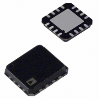
ADA4937-1YCPZ-R7 Analog Devices Inc, ADA4937-1YCPZ-R7 Datasheet - Page 18

ADA4937-1YCPZ-R7
Manufacturer Part Number
ADA4937-1YCPZ-R7
Description
IC ADC DRIVER DIFF 16-LFCSP
Manufacturer
Analog Devices Inc
Type
ADC Driverr
Datasheet
1.ADA4937-1YCPZ-R7.pdf
(28 pages)
Specifications of ADA4937-1YCPZ-R7
Design Resources
Driving AD9233/46/54 ADCs in AC-Coupled Baseband Appls (CN0051)
Applications
Data Acquisition
Mounting Type
Surface Mount
Package / Case
16-LFCSP
No. Of Amplifiers
1
Input Offset Voltage
2.5mV
Bandwidth
1.9GHz
Slew Rate
6000V/µs
Supply Voltage Range
3V To 5.25V
Supply Current
39.5mA
Amplifier Case Style
LFCSP
No. Of Pins
16
Rohs Compliant
Yes
Lead Free Status / RoHS Status
Lead free / RoHS Compliant
Other names
ADA4937-1YCPZ-R7TR
Available stocks
Company
Part Number
Manufacturer
Quantity
Price
Company:
Part Number:
ADA4937-1YCPZ-R7
Manufacturer:
AD
Quantity:
5 015
ADA4937-1/ADA4937-2
THEORY OF OPERATION
The ADA4937-x differs from conventional op amps in that it
has two outputs whose voltages move in opposite directions.
Like an op amp, it relies on open-loop gain and negative feed-
back to force these outputs to the desired voltages. The ADA4937-x
behaves much like a standard voltage feedback op amp, which
makes it easier to perform single-ended-to-differential conversions,
common-mode level shifting, and amplifications of differential
signals. Also like an op amp, the ADA4937-x has high input
impedance and low output impedance.
Two feedback loops control the differential and common-mode
output voltages. The differential feedback loop, set with external
resistors, controls only the differential output voltage. The
common-mode feedback loop controls only the common-mode
output voltage. This architecture makes it easy to set the output
common-mode level to any arbitrary value. It is forced, by
internal common-mode feedback, to be equal to the voltage
applied to the V
output voltage.
The ADA4937-x architecture results in outputs that are highly
balanced over a wide frequency range without requiring tightly
matched external components. The common-mode feedback
loop forces the signal component of the output common-mode
voltage to zero. This results in nearly perfectly balanced differential
outputs that are identical in amplitude and are exactly 180° apart
in phase.
ANALYZING AN APPLICATION CIRCUIT
The ADA4937-x uses open-loop gain and negative feedback to
force its differential and common-mode output voltages in such
a way as to minimize the differential and common-mode error
voltages. The differential error voltage is defined as the voltage
between the differential inputs labeled +IN and −IN (see
Figure 52). For most purposes, this voltage can be assumed
to be zero. Similarly, the difference between the actual output
common-mode voltage and the voltage applied to V
also be assumed to be zero. Starting from these two assumptions,
any application circuit can be analyzed.
Table 9. Output Noise Voltage Density Calculations
Input Noise Contribution
Differential Input
Inverting Input
Noninverting Input
V
Gain Resistor R
Gain Resistor R
Feedback Resistor R
Feedback Resistor R
OCM
Input
G1
G2
OCM
F1
F2
input without affecting the differential
Input Noise Term
v
i
i
v
v
v
v
v
nIN−
nIN+
nIN
n, cm
nRG1
nRG2
nRF1
nRF2
OCM
can
Input Noise
Voltage Density
v
i
i
v
(4kTR
(4kTR
(4kTR
(4kTR
nIN−
nIN+
nIN
n, cm
Rev. C | Page 18 of 28
× (R
× (R
G1
G2
F1
F2
)
)
)
)
1/2
1/2
1/2
1/2
G2
G1
||R
||R
F2
F1
)
)
SETTING THE CLOSED-LOOP GAIN
The differential-mode gain of the circuit in Figure 52 can be
determined by
This assumes that the input resistors (R
(R
ESTIMATING THE OUTPUT NOISE VOLTAGE
The differential output noise of the ADA4937-x can be esti-
mated using the noise model in Figure 53. The input-referred
noise voltage density, v
the noise currents, i
ground. The noise currents are assumed to be equal and produce
a voltage across the parallel combination of the gain and feedback
resistances. v
of the four resistors contributes (4kTR
Table 9 summarizes the input noise sources, the multiplication
factors, and the output-referred noise density terms.
F
) on each side are equal.
V
V
Output
Multiplication Factor
G
G
G
G
G
G
1
1
OUT
IN
N
N
N
N
N
N
(β
(1 − β
(1 − β
,
dm
,
dm
1
V
V
n, cm
− β
nRG1
nRG2
=
1
2
2
)
)
is the noise voltage density at the V
)
R
R
Figure 53. ADA4937-x Noise Model
R
R
G
F
i
i
G1
G2
nIN+
nIN–
nIN−
nIN
and i
, is modeled as a differential input, and
V
nIN
R
R
nIN+
F1
F2
ADA4937
+
, appear between each input and
V
V
V
nRF1
OCM
nRF2
Output Noise
Voltage Density Term
v
v
v
v
v
v
v
v
nO1
nO2
nO3
nO4
nO5
nO6
nO7
nO8
x
)
G
1/2
= G
= G
= G
= G
= G
= G
= (4kTR
= (4kTR
) and feedback resistors
.
N
N
N
N
N
N
V
(v
[i
[i
(β
(1 − β
(1 − β
nOD
nIN−
nIN+
V
nIN
1
nCM
F1
F2
− β
)
)
)
× (R
× (R
1/2
1/2
1
2
OCM
)(4kTR
)(4kTR
2
)(v
G2
G1
n, cm
pin. Each
||R
||R
G1
G2
F2
F1
)
)]
)]
)
)
1/2
1/2


