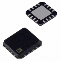
ADA4937-1YCPZ-R7 Analog Devices Inc, ADA4937-1YCPZ-R7 Datasheet - Page 19

ADA4937-1YCPZ-R7
Manufacturer Part Number
ADA4937-1YCPZ-R7
Description
IC ADC DRIVER DIFF 16-LFCSP
Manufacturer
Analog Devices Inc
Type
ADC Driverr
Datasheet
1.ADA4937-1YCPZ-R7.pdf
(28 pages)
Specifications of ADA4937-1YCPZ-R7
Design Resources
Driving AD9233/46/54 ADCs in AC-Coupled Baseband Appls (CN0051)
Applications
Data Acquisition
Mounting Type
Surface Mount
Package / Case
16-LFCSP
No. Of Amplifiers
1
Input Offset Voltage
2.5mV
Bandwidth
1.9GHz
Slew Rate
6000V/µs
Supply Voltage Range
3V To 5.25V
Supply Current
39.5mA
Amplifier Case Style
LFCSP
No. Of Pins
16
Rohs Compliant
Yes
Lead Free Status / RoHS Status
Lead free / RoHS Compliant
Other names
ADA4937-1YCPZ-R7TR
Available stocks
Company
Part Number
Manufacturer
Quantity
Price
Company:
Part Number:
ADA4937-1YCPZ-R7
Manufacturer:
AD
Quantity:
5 015
Similar to the case of a conventional op amp, the output noise
voltage densities can be estimated by multiplying the input-
referred terms at +IN and −IN by the appropriate output factor,
where:
When R
becomes
Note that the output noise from V
The total differential output noise density, v
square of the individual output noise terms.
IMPACT OF MISMATCHES IN THE FEEDBACK
NETWORKS
As previously mentioned in the Setting the Closed-Loop Gain
section), even if the external feedback networks (R
mismatched, the internal common-mode feedback loop still
forces the outputs to remain balanced. The amplitudes of the
signals at each output remain equal and 180° out of phase. The
input-to-output differential mode gain varies proportionately to
the feedback mismatch, but the output balance is unaffected.
As well as causing a noise contribution from V
errors in the external resistors result in a degradation of the
ability of the circuit to reject input common-mode signals, much
the same as for a four-resistor difference amplifier made from
a conventional op amp.
In addition, if the dc levels of the input and output common-
mode voltages are different, matching errors result in a small
differential-mode output offset voltage. When G = 1, with a
ground referenced input signal and the output common-mode
level set to 2.5 V, an output offset of as much as 25 mV (1%
of the difference in common-mode levels) can result if 1% toler-
ance resistors are used. Resistors of 1% tolerance result in a
worst-case input CMRR of approximately 40 dB, a worst-case
differential-mode output offset of 25 mV due to 2.5 V level
shift, and no significant degradation in output balance error.
CALCULATING THE INPUT IMPEDANCE FOR AN
APPLICATION CIRCUIT
The effective input impedance of a circuit depends on whether
the amplifier is being driven by a single-ended or differential
signal source. For balanced differential input signals, as shown
in Figure 54, the input impedance (R
(+D
G
β
1
N
=
=
IN
G
v
R
(
nOD
and −D
N
F1
β
R
1
F1
=
+
G1
+
/R
2
=
R
1
β
β
G1
G1
2
=
∑
)
i
IN
= R
=
8
1
1
and
) is simply R
is the circuit noise gain.
v
+
nOi
2
F2
R
R
/R
G
F
β
2
G2
=
, then β1 = β2 = β, and the noise gain
R
F2
IN, dm
R
+
G2
R
= 2 × R
G2
OCM
are the feedback factors.
IN, dm
goes to zero in this case.
G
) between the inputs
.
nOD
OCM
, is the root-sum-
F
, ratio matching
/R
G
) are
Rev. C | Page 19 of 28
For an unbalanced, single-ended input signal (see Figure 55),
the input impedance is
The input impedance of the circuit is effectively higher than it
would be for a conventional op amp connected as an inverter
because a fraction of the differential output voltage appears at
the inputs as a common-mode signal, partially bootstrapping
the voltage across the Input Gain Resistor R
Terminating a Single-Ended Input
This section explains how to properly terminate a single-ended
input to the ADA4937-x. Using a simple example with an input
source of 2 V and a source resistor of 50 Ω, four simple steps
must be followed.
1.
Figure 55. ADA4937-x Configured for Unbalanced (Single-Ended) Input
Figure 54. ADA4937-x Configured for Balanced (Differential) Inputs
The input impedance must be calculated using the formula
R
R
IN
IN
V
2V
S
,
=
cm
R
+D
–D
1
50Ω
=
S
R
Figure 56. Single-Ended Input Impedance R
−
IN
IN
S
2
1
R
R
×
267Ω
−
R
T
S
R
R
R
(
IN
2
R
G
G
G
R
G
×
F
+
(
R
R
V
R
R
200Ω
V
200Ω
G
G
R
OCM
R
R
R
T
R
OCM
+IN
–IN
G
G
G
G
F
F
V
ADA4937-1/ADA4937-2
+
)
ADA4937
OCM
R
+V
=
R
R
F
S
F
F
)
R
R
ADA4937
1
F
F
200Ω
200Ω
ADA4937
−
R
R
+V
F
F
+V
–V
2
S
×
S
S
(
200
200
200
V
G
OUT, dm
.
+
200
V
OUT, dm
IN
)
R
L
=
267
V
O
Ω


