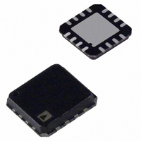
ADA4937-1YCPZ-R7 Analog Devices Inc, ADA4937-1YCPZ-R7 Datasheet - Page 22

ADA4937-1YCPZ-R7
Manufacturer Part Number
ADA4937-1YCPZ-R7
Description
IC ADC DRIVER DIFF 16-LFCSP
Manufacturer
Analog Devices Inc
Type
ADC Driverr
Datasheet
1.ADA4937-1YCPZ-R7.pdf
(28 pages)
Specifications of ADA4937-1YCPZ-R7
Design Resources
Driving AD9233/46/54 ADCs in AC-Coupled Baseband Appls (CN0051)
Applications
Data Acquisition
Mounting Type
Surface Mount
Package / Case
16-LFCSP
No. Of Amplifiers
1
Input Offset Voltage
2.5mV
Bandwidth
1.9GHz
Slew Rate
6000V/µs
Supply Voltage Range
3V To 5.25V
Supply Current
39.5mA
Amplifier Case Style
LFCSP
No. Of Pins
16
Rohs Compliant
Yes
Lead Free Status / RoHS Status
Lead free / RoHS Compliant
Other names
ADA4937-1YCPZ-R7TR
Available stocks
Company
Part Number
Manufacturer
Quantity
Price
Company:
Part Number:
ADA4937-1YCPZ-R7
Manufacturer:
AD
Quantity:
5 015
ADA4937-1/ADA4937-2
LAYOUT, GROUNDING, AND BYPASSING
As a high speed device, the ADA4937-x is sensitive to the
PCB environment in which it operates. Realizing its superior
performance requires attention to the details of high speed
PCB design. This section shows a detailed example of how
the design issues of the ADA4937-1 were addressed.
The first requirement is a solid ground plane that covers as
much of the board area around the ADA4937-1 as possible.
However, the area near the feedback resistors (R
resistors (R
should be cleared of all ground and power planes (see Figure 61).
Clearing the ground and power planes minimizes any stray capa-
citance at these nodes and prevents peaking of the response of
the amplifier at high frequencies.
The thermal resistance, θ
the exposed pad, soldered to a high thermal conductivity 4-layer
circuit board, as described in EIA/JESD 51-7.
Figure 61. Ground and Power Plane Voiding in Vicinity of R
G
), and the input summing nodes (Pin 2 and Pin 3)
Figure 63. Cross-Section of 4-layer PCB Showing Thermal Via Connection to Buried Ground Plane (Dimensions in mm)
JA
, is specified for the device, including
GROUND PLANE
BOTTOM METAL
POWER PLANE
TOP METAL
F
), input gain
F
and R
G
Rev. C | Page 22 of 28
VIA HOLE
PLATED
1.30
0.30
Bypass the power supply pins as close to the device as possible
and directly to a nearby ground plane. Use high frequency ceramic
chip capacitors. It is recommended that two parallel bypass capaci-
tors (1000 pF and 0.1 µF) be used for each supply with the 1000 pF
capacitor placed closer to the device; further away, provide low
frequency bypassing using 10 µF tantalum capacitors from each
supply to ground.
Signal routing should be short and direct to avoid parasitic
effects. Wherever complementary signals exist, provide a sym-
metrical layout to maximize balanced performance. When
routing differential signals over a long distance, keep PCB
traces close together and twist any differential wiring to mini-
mize loop area. Doing this reduces radiated energy and makes
the circuit less susceptible to interference.
Figure 62. Recommended PCB Thermal Attach Pad Dimensions (mm)
1.30
0.80
1.30
0.80


