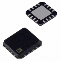
ADA4937-1YCPZ-R7 Analog Devices Inc, ADA4937-1YCPZ-R7 Datasheet - Page 20

ADA4937-1YCPZ-R7
Manufacturer Part Number
ADA4937-1YCPZ-R7
Description
IC ADC DRIVER DIFF 16-LFCSP
Manufacturer
Analog Devices Inc
Type
ADC Driverr
Datasheet
1.ADA4937-1YCPZ-R7.pdf
(28 pages)
Specifications of ADA4937-1YCPZ-R7
Design Resources
Driving AD9233/46/54 ADCs in AC-Coupled Baseband Appls (CN0051)
Applications
Data Acquisition
Mounting Type
Surface Mount
Package / Case
16-LFCSP
No. Of Amplifiers
1
Input Offset Voltage
2.5mV
Bandwidth
1.9GHz
Slew Rate
6000V/µs
Supply Voltage Range
3V To 5.25V
Supply Current
39.5mA
Amplifier Case Style
LFCSP
No. Of Pins
16
Rohs Compliant
Yes
Lead Free Status / RoHS Status
Lead free / RoHS Compliant
Other names
ADA4937-1YCPZ-R7TR
Available stocks
Company
Part Number
Manufacturer
Quantity
Price
Company:
Part Number:
ADA4937-1YCPZ-R7
Manufacturer:
AD
Quantity:
5 015
ADA4937-1/ADA4937-2
2.
3.
R
which would be the case if the termination were not affected by
the amplifier circuit.
4.
TS
= R
V
2V
b.
For the source termination to be 50 Ω, the termination
resistor (R
makes R
To compensate for the imbalance of the gain resistors,
a correction resistor (R
inverting Input Gain Resistor R
Thevenin equivalent of the Source Resistance R
The feedback resistor is calculated to adjust the output
voltage.
a.
S
R
R
F
F
TH
1.1V
V
=
To make V
input termination, R
=
50Ω
TH
To make the output voltage V
calculated using the following formula:
R
= R
S
V
V
V
2V
T
OUT
S
S
Figure 58. Calculating Thevenin Equivalent
||R
OUT
equal to 61.9 Ω.
50Ω
Figure 57. Adding Termination Resistor R
T
27.4Ω
27.4Ω
) is calculated using R
R
Figure 59. Balancing Gain Resistor R
R
T
TH
×
TS
50Ω
= 27.4 Ω. Note that V
×
R
V
61.9Ω
(
S
O
V
R
(
TH
R
= V
TH
R
G
200Ω
V
200Ω
G
T
R
R
OCM
G
G
+
R
61.9Ω
+
S
T
R
= 2 V to recover the loss due to the
R
200Ω
200Ω
TS
V
TS
R
R
TS
OCM
) is added in series with the
F
G
G
)
should be
)
=
200Ω
ADA4937
200Ω
R
R
=
F
F
+V
–V
1
G
S
S
. R
×
2
T
200Ω
200Ω
ADA4937
1.1V
||R
V
R
R
OUT
×
(
TH
TS
TH
200
F
F
+V
–V
(
IN
is equal to the
200
1
S
S
is not equal to V
= 1 V, R
1 .
= 50 Ω, which
27.4Ω
1
+
R
1 .
TH
+
G
27
27
T
R
.
) 4
L
F
.
) 4
must be
S
V
0.97V
||R
O
=
R
207
L
T
=
.
414
V
S
Ω
/2,
O
Rev. C | Page 20 of 28
Ω
INPUT COMMON-MODE VOLTAGE RANGE IN
SINGLE-SUPPLY APPLICATIONS
The ADA4937-x is optimized for level-shifting ground-referenced
input signals. As such, the center of the input common-mode
range is shifted approximately 1 V down from midsupply. For
5 V single-supply operation, the input common-mode range at
the summing nodes of the amplifier is 0.3 V to 3.0 V, and 0.3 V
to 1.2 V with a 3.3 V supply. To avoid clipping at the outputs,
the voltage swing at the +IN and −IN terminals must be confined
to these ranges.
SETTING THE OUTPUT COMMON-MODE VOLTAGE
The V
approximately equal to the midsupply point, [(+V
Relying on this internal bias results in an output common-mode
voltage that is within about 100 mV of the expected value.
In cases where more accurate control of the output common-
mode level is required, it is recommended that an external source,
or resistor divider (10 kΩ or greater resistors), be used. The
output common-mode offset listed in Table 2 and Table 4 assumes
that the V
It is also possible to connect the V
level (CML) output of an ADC. However, care must be taken to
ensure that the output has sufficient drive capability. The input
impedance of the V
ADA4937-x devices share one reference output, it is recommended
that a buffer be used.
Table 10 and Table 11 list several common gain settings, asso-
ciated resistor values, input impedances, and output noise density
values for both balanced and unbalanced input configurations.
POWER-DOWN OPERATION
The ADA4937-x power-down pin features an internal 25 kΩ
pull-up resistor to the positive supply (+V
with the power-down pin left unconnected (floating), the
ADA4937-x turns on. Applying a voltage of ≤1 V turns the
ADA4937-x off.
OCM
V
2V
S
Figure 60. Complete Single-Ended-to-Differential System
OCM
pin of the ADA4937-x is internally biased at a voltage
50Ω
R
S
input is driven by a low impedance voltage source.
61.9Ω
27.4Ω
OCM
R
R
TS
T
pin is approximately 10 kΩ. If multiple
200Ω
200Ω
V
R
R
OCM
G
G
OCM
ADA4937
R
R
F
F
input to a common-mode
+V
–V
S
S
S
). This ensures that,
S
) + (−V
R
L
V
O
S
)]/2.


