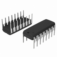
SA571NG ON Semiconductor, SA571NG Datasheet - Page 5

SA571NG
Manufacturer Part Number
SA571NG
Description
IC COMPANDOR DUAL GAIN 16-DIP
Manufacturer
ON Semiconductor
Type
Compandorr
Datasheet
1.SA571NG.pdf
(11 pages)
Specifications of SA571NG
Applications
Cellular Radio, Players
Mounting Type
Through Hole
Package / Case
16-DIP (0.300", 7.62mm)
Product
General Purpose Audio Amplifiers
Operating Supply Voltage
6 V to 18 V
Supply Current
4.2 mA
Maximum Power Dissipation
400 mW
Maximum Operating Temperature
+ 85 C
Mounting Style
Through Hole
Minimum Operating Temperature
- 40 C
Supply Voltage (max)
18 V
Supply Voltage (min)
6 V
Operating Temperature (min)
-40C
Operating Temperature (max)
85C
Operating Temperature Classification
Industrial
Mounting
Through Hole
Pin Count
16
Package Type
PDIP
Lead Free Status / RoHS Status
Lead free / RoHS Compliant
Other names
SA571NG
SA571NGOS
SA571NGOS
Available stocks
Company
Part Number
Manufacturer
Quantity
Price
Company:
Part Number:
SA571NG
Manufacturer:
BCD
Quantity:
12 000
Part Number:
SA571NG
Manufacturer:
ON/安森美
Quantity:
20 000
electronic
applications,
transconductance amplifier can be used, but when
high−performance is required, one has to resort to complex
discrete circuitry with many expensive, well−matched
components. This paper describes an inexpensive integrated
circuit, the SA571 Compandor, which offers a pair of high
performance gain control circuits featuring low distortion
(<0.1%), high signal−to−noise ratio (90 dB), and wide
dynamic range (110 dB).
Circuit Background
the requirements of the telephone system. When several
telephone channels are multiplexed onto a common line, the
resulting signal−to−noise ratio is poor and companding is
used to allow a wider dynamic range to be passed through
the channel. Figure 4 graphically shows what a compandor
can do for the signal−to−noise ratio of a restricted dynamic
range channel. The input level range of +20 to −80 dB is
shown undergoing a 2−to−1 compression where a 2.0 dB
input level change is compressed into a 1.0 dB output level
change by the compressor. The original 100 dB of dynamic
range is thus compressed to a 50 dB range for transmission
through
complementary expansion on the receiving end restores the
original signal levels and reduces the channel noise by as
much as 45 dB.
the rectifier and the gain control element. The phone system
Much interest has been expressed in high performance
The SA571 Compandor was originally designed to satisfy
The significant circuits in a compressor or expander are
Figure 4. Restricted Dynamic Range Channel
LEVEL
INPUT
+20
0dB
−40
−80
a
gain
restricted
an
INTRODUCTION
control
integrated
NOISE
dynamic
circuits.
circuit
range
For
OUTPUT
LEVEL
channel.
0dB
non−critical
−20
−40
−80
operational
http://onsemi.com
A
SA571
5
requires a simple full−wave averaging rectifier with good
accuracy, since the rectifier accuracy determines the (input)
output level tracking accuracy. The gain cell determines the
distortion and noise characteristics, and the phone system
specifications here are very loose. These specs could have
been met with a simple Operational Transconductance
Multiplier, or OTA, but the gain of an OTA is proportional
to temperature and this is very undesirable. Therefore, a
linearized transconductance multiplier was designed which
is insensitive to temperature and offers low noise and low
distortion performance. These features make the circuit
useful in audio and data systems as well as in
telecommunications systems.
Basic Hook−up and Operation
(there are two identical channels on the IC). The full−wave
averaging rectifier provides a gain control current, I
variable gain (DG) cell. The output of the DG cell is a current
which is fed to the summing node of the operational
amplifier. Resistors are provided to establish circuit gain and
set the output DC bias.
systems, so the internal summing nodes must be biased at
some voltage above ground. An internal band gap voltage
reference provides a very stable, low noise 1.8 V reference
denoted V
to V
(located at the right of R
The THD trim pin is also at the V
Figure 5 shows the block diagram of one half of the chip,
The circuit is intended for use in single power supply
RECT
REF
Figure 5. Chip Block Diagram (1 of 2 Channels)
G
3,14
2,15
IN
, and the summing nodes of the rectifier and DG cell
IN
REF
20kW
10kW
R
R
. The non−inverting input of the op amp is tied
THD TRIM
2
1
C
DG
RECT
IG
1,16
8,9
1
20kW
and R
R
3
30kW
R
R
3
4
2
6,11
) have the same potential.
REF
INV
V
1.8V
IN
REF
potential.
5,12
V
GND PIN 4
CC
−
+
PIN 13
OUTPUT
G
7,10
, for the


