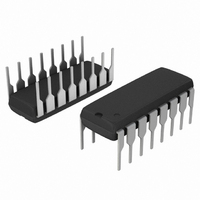
SA571NG ON Semiconductor, SA571NG Datasheet - Page 7

SA571NG
Manufacturer Part Number
SA571NG
Description
IC COMPANDOR DUAL GAIN 16-DIP
Manufacturer
ON Semiconductor
Type
Compandorr
Datasheet
1.SA571NG.pdf
(11 pages)
Specifications of SA571NG
Applications
Cellular Radio, Players
Mounting Type
Through Hole
Package / Case
16-DIP (0.300", 7.62mm)
Product
General Purpose Audio Amplifiers
Operating Supply Voltage
6 V to 18 V
Supply Current
4.2 mA
Maximum Power Dissipation
400 mW
Maximum Operating Temperature
+ 85 C
Mounting Style
Through Hole
Minimum Operating Temperature
- 40 C
Supply Voltage (max)
18 V
Supply Voltage (min)
6 V
Operating Temperature (min)
-40C
Operating Temperature (max)
85C
Operating Temperature Classification
Industrial
Mounting
Through Hole
Pin Count
16
Package Type
PDIP
Lead Free Status / RoHS Status
Lead free / RoHS Compliant
Other names
SA571NG
SA571NGOS
SA571NGOS
Available stocks
Company
Part Number
Manufacturer
Quantity
Price
Company:
Part Number:
SA571NG
Manufacturer:
BCD
Quantity:
12 000
Part Number:
SA571NG
Manufacturer:
ON/安森美
Quantity:
20 000
amp is a one−stage op amp, biased so that only one output
device is on at a time. The non−inverting input, (the base of
Q
1.8 V, V
(the emitters of Q
R
that only one device is on at a time. To detect the output
current of the op amp, we simply use the collector currents
of the output devices Q
input swings positive and Q
swings negative. The collector currents will be in error by
the a of Q
respectively. ICs such as this have typical NPN b’s of 200
and PNP b’s of 40. The a’s of 0.995 and 0.975 will produce
errors of 0.5% on negative swings and 2.5% on positive
swings. The 1.5% average of these errors yields a mere 0.13
dB gain error.
(typically 50 nA), will become significant as it must be
supplied by Q
coupling into the rectifier. If an offset voltage exists between
the V
V
cause an input current of 100 nA which will produce twice
1
1
OS
Figure 9 shows the rectifier circuit in more detail. The op
At very low input signal levels the bias current of Q
. The single diode between the bases of Q
), which is shown grounded, is actually tied to the internal
/R
Q
IN
1
1
Figure 9. Simplified Rectifier Schematic
REF
Q
input pin and the base of Q
will be generated. A mere 1.0 mV of offset will
2
Q
I
1
5
. The inverting input is tied to the op amp output,
3
or Q
5
. Another low level error can be caused by DC
NOTE:
Q
V+
V−
5
6
D
4
I
and Q
2
1
on negative or positive signal swings,
I
5
G
and Q
6
), and the input summing resistor
+ 2
Q
6
5
Q
6
V
. Q
5
conducts when the input
IN
R 1
Q
avg
6
7
will conduct when the
C
10kW
2
R
, an error current of
R
10kW
1
R
S
5
and Q
Q
8
V
IN
6
assures
http://onsemi.com
Q
9
2
,
SA571
7
the error of the input bias current. For highest accuracy, the
rectifier should be coupled capacitively. At high input levels
the b of the PNP Q
increasing error until the circuit saturates. Saturation can be
avoided by limiting the current into the rectifier input to
250 mA. If necessary, an external resistor may be placed in
series with R
shows the rectifier accuracy vs. input level at a frequency of
1.0 kHz.
fall off. The roll−off will be more pronounced at lower input
levels due to the increasing amount of gain required to
switch between Q
frequency response for input levels of 0 dBm, −20 dBm, and
−40 dBm is shown in Figure 11. The response at all three
levels is flat to well above the audio range.
At very high frequencies, the response of the rectifier will
Figure 11. Rectifier Frequency Response vs.
0
3
+1
−1
1
Figure 10. Rectifier Accuracy
0
to limit the current to this value. Figure 10
6
will begin to suffer, and there will be an
RECTIFIER INPUT dBm
10k
5
−40dBm
FREQUENCY (Hz)
−40
or Q
Input Level
6
−20
conducting. The rectifier
INPUT = 0dBm
1MEG
0
−20dBm


