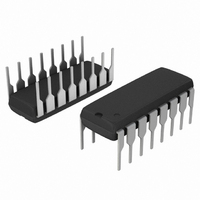
SA571NG ON Semiconductor, SA571NG Datasheet - Page 9

SA571NG
Manufacturer Part Number
SA571NG
Description
IC COMPANDOR DUAL GAIN 16-DIP
Manufacturer
ON Semiconductor
Type
Compandorr
Datasheet
1.SA571NG.pdf
(11 pages)
Specifications of SA571NG
Applications
Cellular Radio, Players
Mounting Type
Through Hole
Package / Case
16-DIP (0.300", 7.62mm)
Product
General Purpose Audio Amplifiers
Operating Supply Voltage
6 V to 18 V
Supply Current
4.2 mA
Maximum Power Dissipation
400 mW
Maximum Operating Temperature
+ 85 C
Mounting Style
Through Hole
Minimum Operating Temperature
- 40 C
Supply Voltage (max)
18 V
Supply Voltage (min)
6 V
Operating Temperature (min)
-40C
Operating Temperature (max)
85C
Operating Temperature Classification
Industrial
Mounting
Through Hole
Pin Count
16
Package Type
PDIP
Lead Free Status / RoHS Status
Lead free / RoHS Compliant
Other names
SA571NG
SA571NGOS
SA571NGOS
Available stocks
Company
Part Number
Manufacturer
Quantity
Price
Company:
Part Number:
SA571NG
Manufacturer:
BCD
Quantity:
12 000
Part Number:
SA571NG
Manufacturer:
ON/安森美
Quantity:
20 000
The maximum output level before clipping occurs in the
gain cell is plotted along with the output noise in a 20 kHz
bandwidth. Note that the noise drops as the gain is reduced
for the first 20 dB of gain reduction. At high gains, the signal
to noise ratio is 90 dB, and the total dynamic range from
maximum signal to minimum noise is 110 dB.
imperfect device matching and mismatches in the current
sources, I
I
effective in nulling out any control signal feedthrough, but
in general, the null for minimum feedthrough will be
different than the null in distortion. The control signal
feedthrough can be trimmed independently of distortion by
tying a current source to the DG input pin. This effectively
trims I
†For information on tape and reel specifications, including part orientation and tape sizes, please refer to our Tape and Reel Packaging
G
ORDERING INFORMATION
Specifications Brochure, BRD8011/D.
SA571D
SA571DG
SA571DR2
SA571DR2G
SA571N
SA571NG
Figure 15 shows the noise performance of the DG cell.
Control signal feedthrough is generated in the gain cell by
will cause a small output signal. The distortion trim is
1
. Figure 16 shows such a trim network.
Device
1
−100
and I
+20
−20
−40
−60
−80
0
−40
Figure 15. Dynamic Range
2
. When no input signal is present, changing
110dB
VCA GAIN (0dB)
−20
16−Pin Plastic Small Outline (SO−16 WB) Package
16−Pin Plastic Small Outline (SO−16 WB) Package
16−Pin Plastic Small Outline (SO−16 WB) Package
16−Pin Plastic Small Outline (SO−16 WB) Package
SIGNAL LEVEL
16−Pin Plastic Dual In−Line Package (PDIP−16)
16−Pin Plastic Dual In−Line Package (PDIP−16)
MAXIMUM
0
20kHz BW
NOISE IN
90dB
Description
(Pb−Free)
(Pb−Free)
(Pb−Free)
http://onsemi.com
SA571
9
Operation Amplifier
equivalent to a 741 with a 1.0 MHz bandwidth. Figure 17
shows the basic circuit. Split collectors are used in the input
pair to reduce g
just 10 pF may be used. The output stage, although capable
of output currents in excess of 20 mA, is biased for a low
quiescent current to conserve power. When driving heavy
loads, this leads to a small amount of crossover distortion.
The main op amp shown in the chip block diagram is
−IN
Figure 17. Operational Amplifier
Figure 16. Control Signal Feedthrough
Q
100kW
Temperature Range
3
Q
M
1
−40 to +85°C
−40 to +85°C
−40 to +85°C
−40 to +85°C
−40 to +85°C
−40 to +85°C
, so that a small compensation capacitor of
V
CC
I
Q
R−SELECT FOR
1
Q
2
4
3.6V
470kW
+IN
C
C
Q
D
D
2
I
2
1
2
TO PIN 3 OR 14
1000 / Tape & Reel
1000 / Tape & Reel
Q
6
47 Units / Rail
47 Units / Rail
25 Units / Rail
25 Units / Rail
Shipping
OUT
†


