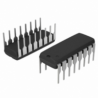
SA571NG ON Semiconductor, SA571NG Datasheet - Page 8

SA571NG
Manufacturer Part Number
SA571NG
Description
IC COMPANDOR DUAL GAIN 16-DIP
Manufacturer
ON Semiconductor
Type
Compandorr
Datasheet
1.SA571NG.pdf
(11 pages)
Specifications of SA571NG
Applications
Cellular Radio, Players
Mounting Type
Through Hole
Package / Case
16-DIP (0.300", 7.62mm)
Product
General Purpose Audio Amplifiers
Operating Supply Voltage
6 V to 18 V
Supply Current
4.2 mA
Maximum Power Dissipation
400 mW
Maximum Operating Temperature
+ 85 C
Mounting Style
Through Hole
Minimum Operating Temperature
- 40 C
Supply Voltage (max)
18 V
Supply Voltage (min)
6 V
Operating Temperature (min)
-40C
Operating Temperature (max)
85C
Operating Temperature Classification
Industrial
Mounting
Through Hole
Pin Count
16
Package Type
PDIP
Lead Free Status / RoHS Status
Lead free / RoHS Compliant
Other names
SA571NG
SA571NGOS
SA571NGOS
Available stocks
Company
Part Number
Manufacturer
Quantity
Price
Company:
Part Number:
SA571NG
Manufacturer:
BCD
Quantity:
12 000
Part Number:
SA571NG
Manufacturer:
ON/安森美
Quantity:
20 000
Variable Gain Cell
linearized two−quadrant transconductance multiplier. Q
Q
gain control pair, Q
a current mirror provides the output current.
ground potential (V
input current I
Q
been set at twice the value of I
Q
This drive signal will be linear for small signals, but very
non−linear for large signals, since it is compensating for the
non−linearity of the differential pair, Q
signal conditions.
signal is applied to the gain control pair, Q
two differential pairs of transistors have the same signal
applied, their collector current ratios will be identical
regardless of the magnitude of the currents. This gives us:
plus the relationships I
yield the multiplier transfer function,
V
2
1
1
Figure 12 is a diagram of the variable gain cell. This is a
IN
The op amp maintains the base and collector of Q
The op amp has thus forced a linear current swing between
The key to the circuit is that this same predistorted drive
and the op amp provide a predistorted drive signal for the
along with the current I
and Q
20k
R
2
140mA
Figure 12. Simplified DG Cell Schematic
I
IN
2
I
1
by providing the proper drive to the base of Q
IN
Q
NOTE:
I
1
2
(= V
I
− (I
OUT
I
I
3
C1
C2
REF
and Q
I
2
280mA
1
Q
IN
+
G
I
(= 2I
+
+ I
OUT
2
) by controlling the base of Q
/R
= I
IN
I
I
4
I
I
2
C4
C3
1
C3
G
1
. The gain is controlled by I
1
) = I
+
) is thus forced to flow through
)
, so I
I
+ I
+
IN
I
I
1
G
+
1
−
1
, the current through Q
C4
+
− I
I
C1
I
I
V+
V−
IN
1
1
and I
IN
) I
* I
V
= I
R
+
= I
IN
2
1
IN
IN
1
I
I
I
and Q
OUT
I
G
C2
G
1
+ I
2
V
R
.
3
IN
IN
2
= I
and Q
Q
. Since I
2
, under large
3
C4
− I
I
4
Q
G
. When
http://onsemi.com
C3
4
2
G
. The
2
2
1
will
and
has
is:
at
1
2
,
.
SA571
8
assumes ideal transistors.
non−linearity is generated, which results in second
harmonic distortion. Figure 13 gives an indication of the
magnitude of the distortion caused by a given input level and
offset voltage. The distortion is linearly proportional to the
magnitude of the offset and the input level. Saturation of the
gain cell occurs at a +8 dBm level. At a nominal operating
level of 0 dBm, a 1.0 mV offset will yield 0.34% of second
harmonic distortion. Most circuits are somewhat better than
this, which means our overall offsets are typically about mV.
The distortion is not affected by the magnitude of the gain
control current, and it does not increase as the gain is
changed. This second harmonic distortion could be
eliminated by making perfect transistors, but since that
would be difficult, we have had to resort to other methods.
A trim pin has been provided to allow trimming of the
internal offsets to zero, which effectively eliminated second
harmonic distortion. Figure 14 shows the simple trim
network required.
This equation is linear and temperature−insensitive, but it
If the transistors are not perfectly matched, a parabolic,
Figure 13. DG Cell Distortion vs. Offset Voltage
.34
4
3
2
1
Figure 14. THD Trim Network
To THD Trim
INPUT LEVEL (dBm)
−6
≈200pF
6.2kW
0
V
CC
20kW
3.6V
+6
R
4mV
3mV
2mV
1mV


