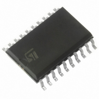
TDA7403DTR STMicroelectronics, TDA7403DTR Datasheet - Page 16

TDA7403DTR
Manufacturer Part Number
TDA7403DTR
Description
IC PROCESSOR BASIC SIGNAL SO-20
Manufacturer
STMicroelectronics
Type
Car Signal Processorr
Datasheet
1.TDA7403D.pdf
(25 pages)
Specifications of TDA7403DTR
Applications
Automotive Systems
Mounting Type
Surface Mount
Package / Case
20-SOIC (7.5mm Width)
Lead Free Status / RoHS Status
Lead free / RoHS Compliant
TDA7403
Automatic Threshold Control
Besides the noise controlled threshold adjust-
ment there is an additional possibility for influenc-
ing the trigger threshold. It is depending on the
stereoblend control.
The point where the MPX signal starts to become
noisy is fixed by the RF part. Therefore also the
starting point of the normal noise-controlled trig-
ger adjustment is fixed (fig. 15). In some cases
the behaviour of the noiseblanker can be im-
proved by increasing the threshold even in a re-
gion of higher fieldstrength. Sometimes a wrong
triggering occures for the MPX signal often shows
distortion in this range which can be avoided
even if using a low threshold.
Because of the overlap of this range and the
range of the stereo/mono transition it can be con-
trolled by stereoblend. This threshold increase is
programmable in 3 steps or switched off with bits
D0 and D1 of the fieldstrength control byte.
Figure 19. Application Example.
16/25
CASS R
CASS L
MPX
AM
=
+V
9V
CC
220nF
100nF
100nF
220nF
100nF
CASS R
CASS L
MPX
AM
V
S
Over Deviation Detector
If the system is tuned to stations with a high de-
viation the noiseblanker can trigger on the higher
frequencies of the modulation. To avoid this
wrong behaviour, which causes noise in the out-
put signal, the noiseblanker offers a deviation de-
pendent threshold adjustment.
By rectifying the MPX signal a further signal rep-
resenting the actual deviation is obtained. It is
used to increase the PEAK voltage. Offset and
gain of this circuit are programmable in 3 steps
with the bits D6 and D7 of the stereodecoder byte
(the first step turns off the detector, see fig. 15).
TEST MODE
During the test mode which can be activated by
setting bit D0 of the testing byte and bit D5 of the
subaddress byte to "1" several internal signals
are available at the CASSR pin.
mode the input resistance of 100kOhm is discon-
nected from the pin. The internal signals available
are shown in the software specification.
CREF
OUTLF
OUTRF
OUTLR
OUTRR
SDA
SCL
SMUTE
LEVEL
GND
10 F
D98AUxx5
During this
OUTRR
OUTRF
OUTLR
SMUTE
OUTLF
LEVEL
SDA
SCL


