TDA7056A NXP Semiconductors, TDA7056A Datasheet - Page 5
TDA7056A
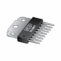
Manufacturer Part Number
TDA7056A
Description
The TDA7056A is a mono BTL output amplifier with DC volume control
Manufacturer
NXP Semiconductors
Datasheet
1.TDA7056A.pdf
(11 pages)
Available stocks
Company
Part Number
Manufacturer
Quantity
Price
Company:

Part Number:
TDA7056A
Manufacturer:
PHILIPS
Quantity:
103
Part Number:
TDA7056A
Manufacturer:
CN/如韵
Quantity:
20 000
Part Number:
TDA7056A/N2
Manufacturer:
PHILIPS/飞利浦
Quantity:
20 000
Part Number:
TDA7056A/N2,112
Manufacturer:
PHILIPS/飞利浦
Quantity:
20 000
Company:
Part Number:
TDA7056AT
Manufacturer:
PHILIPS
Quantity:
5 341
Company:
Part Number:
TDA7056AT
Manufacturer:
PHILIPS
Quantity:
24
Part Number:
TDA7056AT
Manufacturer:
PHI
Quantity:
20 000
Company:
Part Number:
TDA7056AT/N2
Manufacturer:
TI
Quantity:
5 000
Part Number:
TDA7056AT/N2
Manufacturer:
PHILIPS/飞利浦
Quantity:
20 000
Company:
Part Number:
TDA7056AT/N2
Manufacturer:
PHILIPS
Quantity:
16 815


NXP Semiconductors
CHARACTERISTICS
V
Notes to the characteristics
1. With a load connected to the outputs the quiescent current will increase, the maximum value of this increase being
2. The noise output voltage (RMS value) at f = 500 kHz is measured with R
3. The ripple rejection is measured with R
4. The noise output voltage (RMS value) is measured with R
July 1994
V
I
Maximum gain (V
P
THD
G
V
V
B
SVRR
|V
Z
Minimum gain (V
G
V
Mute position
V
DC volume control
φ
I
P
P
5
SYMBOL
I
P
O
I
no(rms)
no(rms)
O
3 W BTL mono audio output amplifier with
DC volume control
v
v
off
= 12 V; f = 1 kHz; R
equal to the DC output offset voltage divided by R
is applied to the positive supply rail.
|
positive supply voltage range
total quiescent current
output power
total harmonic distortion
voltage gain
input signal handling
noise output voltage (RMS value)
bandwidth
supply voltage ripple rejection
DC output offset voltage
input impedance pin 3
voltage gain
noise output voltage (RMS value)
output voltage in mute position
gain control range
control current
5
5
= 0.5 V)
= 1.4 V)
L
= 16 Ω; T
PARAMETER
amb
= 25 °C; unless otherwise specified (see Fig.6)
S
= 0 Ω and f = 100 Hz to 10 kHz. The ripple voltage of 200 mV (RMS value)
L
.
V
THD = 10%; R
THD = 10%; R
P
V
f = 500 kHz; note 2
at −1 dB
note 3
note 4
V
V
P
O
5
5
5
5
= 0.8 V;THD < 1%
≤ 0.3 V; V
= 0 V
= 12 V; R
= 0.5 W
S
CONDITIONS
= 5 kΩ unweighted.
L
I
= 600 mV
= ∞; note 1 −
L
L
= 16 Ω
= 8 Ω
S
= 0 Ω and bandwidth = 5 kHz.
4.5
3
−
−
34.5
0.5
−
−
38
−
15
−
−
−
75
60
MIN.
35.5
46
20
80
70
−
8
3.5
5.2
0.3
0.65
210
20 Hz to
300 kHz
0
−44
20
−
TYP.
Product specificiation
TDA7056A
18
16
−
−
1
36.5
−
−
−
−
150
25
−
30
30
−
80
MAX.
V
mA
W
W
%
dB
V
μV
dB
mV
kΩ
dB
μV
μV
dB
μA
UNIT
Related parts for TDA7056A
Image
Part Number
Description
Manufacturer
Datasheet
Request
R

Part Number:
Description:
NXP Semiconductors designed the LPC2420/2460 microcontroller around a 16-bit/32-bitARM7TDMI-S CPU core with real-time debug interfaces that include both JTAG andembedded trace
Manufacturer:
NXP Semiconductors
Datasheet:

Part Number:
Description:
NXP Semiconductors designed the LPC2458 microcontroller around a 16-bit/32-bitARM7TDMI-S CPU core with real-time debug interfaces that include both JTAG andembedded trace
Manufacturer:
NXP Semiconductors
Datasheet:
Part Number:
Description:
NXP Semiconductors designed the LPC2468 microcontroller around a 16-bit/32-bitARM7TDMI-S CPU core with real-time debug interfaces that include both JTAG andembedded trace
Manufacturer:
NXP Semiconductors
Datasheet:
Part Number:
Description:
NXP Semiconductors designed the LPC2470 microcontroller, powered by theARM7TDMI-S core, to be a highly integrated microcontroller for a wide range ofapplications that require advanced communications and high quality graphic displays
Manufacturer:
NXP Semiconductors
Datasheet:
Part Number:
Description:
NXP Semiconductors designed the LPC2478 microcontroller, powered by theARM7TDMI-S core, to be a highly integrated microcontroller for a wide range ofapplications that require advanced communications and high quality graphic displays
Manufacturer:
NXP Semiconductors
Datasheet:
Part Number:
Description:
The Philips Semiconductors XA (eXtended Architecture) family of 16-bit single-chip microcontrollers is powerful enough to easily handle the requirements of high performance embedded applications, yet inexpensive enough to compete in the market for hi
Manufacturer:
NXP Semiconductors
Datasheet:
Part Number:
Description:
The XA-S3 device is a member of Philips Semiconductors? XA(eXtended Architecture) family of high performance 16-bitsingle-chip microcontrollers
Manufacturer:
NXP Semiconductors
Datasheet:

Part Number:
Description:
The NXP BlueStreak LH75401/LH75411 family consists of two low-cost 16/32-bit System-on-Chip (SoC) devices
Manufacturer:
NXP Semiconductors
Datasheet:
Part Number:
Description:
The NXP LPC3130/3131 combine an 180 MHz ARM926EJ-S CPU core, high-speed USB2
Manufacturer:
NXP Semiconductors
Datasheet:
Part Number:
Description:
The NXP LPC3141 combine a 270 MHz ARM926EJ-S CPU core, High-speed USB 2
Manufacturer:
NXP Semiconductors
Part Number:
Description:
The NXP LPC3143 combine a 270 MHz ARM926EJ-S CPU core, High-speed USB 2
Manufacturer:
NXP Semiconductors

Part Number:
Description:
The NXP LPC3152 combines an 180 MHz ARM926EJ-S CPU core, High-speed USB 2
Manufacturer:
NXP Semiconductors
Part Number:
Description:
The NXP LPC3154 combines an 180 MHz ARM926EJ-S CPU core, High-speed USB 2
Manufacturer:
NXP Semiconductors

Part Number:
Description:
Standard level N-channel enhancement mode Field-Effect Transistor (FET) in a plastic package using NXP High-Performance Automotive (HPA) TrenchMOS technology
Manufacturer:
NXP Semiconductors
Datasheet: