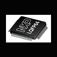
LPC1227FBD64 NXP Semiconductors, LPC1227FBD64 Datasheet - Page 8

LPC1227FBD64
Manufacturer Part Number
LPC1227FBD64
Description
The LPC1227FBD64 is an ARM Cortex-M0 based microcontroller for embedded applications featuring a high level of integration and low power consumption
Manufacturer
NXP Semiconductors
Datasheet
1.LPC1224FBD48.pdf
(61 pages)
Available stocks
Company
Part Number
Manufacturer
Quantity
Price
Company:
Part Number:
LPC1227FBD64
Manufacturer:
AD
Quantity:
31
Part Number:
LPC1227FBD64
Manufacturer:
NXP/恩智浦
Quantity:
20 000
Company:
Part Number:
LPC1227FBD64/301
Manufacturer:
NXP
Quantity:
5 000
Company:
Part Number:
LPC1227FBD64/301
Manufacturer:
NXP
Quantity:
5 000
Part Number:
LPC1227FBD64/301
Manufacturer:
NXP/恩智浦
Quantity:
20 000
Company:
Part Number:
LPC1227FBD64/301,1
Manufacturer:
NXP Semiconductors
Quantity:
10 000
NXP Semiconductors
Table 3.
LPC122X
Product data sheet
Symbol
PIO0_0 to PIO0_31
PIO0_0/RTS0
PIO0_1/RXD0/
CT32B0_CAP0/
CT32B0_MAT0
PIO0_2/TXD0/
CT32B0_CAP1/
CT32B0_MAT1
PIO0_3/DTR0/
CT32B0_CAP2/
CT32B0_MAT2
PIO0_4/DSR0/
CT32B0_CAP3/
CT32B0_MAT3
PIO0_5/DCD0
PIO0_6/RI0/
CT32B1_CAP0/
CT32B1_MAT0
LPC122x pin description
6.2 Pin description
All pins except the supply pins can have more than one function as shown in
pin function is selected through the pin’s IOCON register in the IOCONFIG block. The
multiplexed functions (see
UART receive, transmit, and control functions, and the serial wire debug functions.
For each pin, the default function is listed first together with the pin’s reset state.
15 19
16 20
17 21
18 22
19 23
20 24
21 25
[2]
[3]
[2]
[3]
[2]
[3]
[2]
[3]
[2]
[3]
[2]
[3]
[2]
[3]
Start
logic
input
yes
yes
yes
yes
yes
yes
yes
All information provided in this document is subject to legal disclaimers.
Type Reset
I/O
I/O
O
I/O
I
I
O
I/O
O
I
O
I/O
O
I
O
I/O
I
I
O
I/O
I
I/O
I
I
O
Rev. 2 — 26 August 2011
state
[1]
I; PU
-
I; PU
-
-
-
I; PU
-
-
-
I; PU
-
-
-
I; PU
-
-
-
I; PU
-
I; PU
-
-
-
Table
Description
Port 0 — Port 0 is a 32-bit I/O port with individual direction and
function controls for each bit. The operation of port 0 pins
depends on the function selected through the IOCONFIG
register block.
PIO0_0 — General purpose digital input/output pin.
RTS0 — Request To Send output for UART0.
PIO0_1 — General purpose digital input/output pin.
RXD0 — Receiver input for UART0.
CT32B0_CAP0 — Capture input, channel 0 for 32-bit timer 0.
CT32B0_MAT0 — Match output, channel 0 for 32-bit timer 0.
PIO0_2 — General purpose digital input/output pin.
TXD0 — Transmitter output for UART0.
CT32B0_CAP1 — Capture input, channel 1 for 32-bit timer 0.
CT32B0_MAT1 — Match output, channel 1 for 32-bit timer 0.
PIO0_3 — General purpose digital input/output pin.
DTR0 — Data Terminal Ready output for UART0.
CT32B0_CAP2 — Capture input, channel 2 for 32-bit timer 0.
CT32B0_MAT2 — Match output, channel 2 for 32-bit timer 0.
PIO0_4 — General purpose digital input/output pin.
DSR0 — Data Set Ready input for UART0.
CT32B0_CAP3 — Capture input, channel 3 for 32-bit timer 0.
CT32B0_MAT3 — Match output, channel 3 for 32-bit timer 0.
PIO0_5 — General purpose digital input/output pin.
DCD0 — Data Carrier Detect input for UART0.
PIO0_6 — General purpose digital input/output pin.
RI0 — Ring Indicator input for UART0.
CT32B1_CAP0 — Capture input, channel 0 for 32-bit timer 1.
CT32B1_MAT0 — Match output, channel 0 for 32-bit timer 1.
4) include the counter/timer inputs and outputs, the
32-bit ARM Cortex-M0 microcontroller
LPC122x
© NXP B.V. 2011. All rights reserved.
Table
3. The
8 of 61


