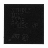
STHDLS101TQTR STMicroelectronics, STHDLS101TQTR Datasheet - Page 16

STHDLS101TQTR
Manufacturer Part Number
STHDLS101TQTR
Description
IC HDMI LEVEL SHIFTER AC 48-QFN
Manufacturer
STMicroelectronics
Type
Level Shifterr
Datasheet
1.STHDLS101TQTR.pdf
(26 pages)
Specifications of STHDLS101TQTR
Function
*
Circuit
*
On-state Resistance
*
Voltage Supply Source
*
Voltage - Supply, Single/dual (±)
*
Current - Supply
*
Operating Temperature
*
Mounting Type
Surface Mount
Package / Case
48-QFN
Applications
Graphic Cards, VGA Interfaces
Maximum Operating Temperature
+ 85 C
Minimum Operating Temperature
- 40 C
Mounting Style
SMD/SMT
Lead Free Status / RoHS Status
Lead free / RoHS Compliant
Other names
497-8499-2
Available stocks
Company
Part Number
Manufacturer
Quantity
Price
Company:
Part Number:
STHDLS101TQTR
Manufacturer:
AD
Quantity:
259
Maximum ratings
5.2
Table 9.
16/26
Symbol
V
T
T
INTRA
INTER
SWING
SKEW-
SKEW-
I
T
V
OFF
T
V
T
JIT
R
H
F
L
Single-ended high
level output voltage
Single-ended low level
output voltage
Single-ended output
swing voltage
Single-ended current
in high-Z state
Rise time
Fall time
Intra-pair differential
skew
Inter-pair lane to lane
output skew
Jitter added to TMDS
signals
TMDS outputs (OUT_D signals)
The level shifter’s TMDS outputs are required to meet the HDMI 1.3 specifications. The
HDMI 1.3 specification is assumed to be the correct reference in instances where this
document conflicts with the HDMI 1.3 specification.
Differential output characteristics for TMDS OUT_D signals
Parameter
AV
voltage in the HDMI or DVI
sink. AV
The open-drain output pulls
down form AV
Swing down from TMDS
termination voltage
(3.3 V ±10%)
Measured with TMDS outputs
pulled up to AV
through 50 Ω resistors
Maximum rise/fall time at
2.7 Gbps = 148ps. 125ps =
148 – 15%
Maximum rise/fall time at
2.7 Gbps = 148 ps.
125ps = 148 – 15%
This differential skew budget
is in addition to the skew
presented between D+ and D-
paired input pins.
This lane to lane skew budget
is in addition to the skew
between differential input
pairs.
Jitter budget for TMDS
signals as they pass through
the level shifter.
7.4 ps = 0.02 Tbit at 2.7 Gbps
CC
is the DC termination
CC
Comments
is nominally 3.3 V
CC
CC
max (3.6 V)
AV
600 mV
400 mV
CC
125 ps
125 ps
AV
Min
-10 mV
CC
-
500 mV
500 mV
AV
AV
Typ
CC
CC
-
AV
400 mV
600 mV
0.4 Tbit
0.4 Tbit
CC
AV
Max
250
7.4
10
10
V
+10 m
CC
STHDLS101T
-
Unit
µA
ps
ps
ps
ps
ps
V
V
V


