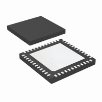
DS16EV5110ASQX/NOPB National Semiconductor, DS16EV5110ASQX/NOPB Datasheet - Page 4

DS16EV5110ASQX/NOPB
Manufacturer Part Number
DS16EV5110ASQX/NOPB
Description
IC EQUALIZER VIDEO 3D+C 48-LLP
Manufacturer
National Semiconductor
Type
Video Equalizerr
Datasheet
1.DS16EV5110ASQXNOPB.pdf
(20 pages)
Specifications of DS16EV5110ASQX/NOPB
Applications
HD Displays, DVI/HDMI
Mounting Type
Surface Mount
Package / Case
48-LLP
Lead Free Status / RoHS Status
Lead free / RoHS Compliant
Other names
DS16EV5110ASQX
www.national.com
LVCMOS DC SPECIFICATIONS
I
I
I
I
V
V
V
V
POWER
PD
N
CML INPUTS
V
V
V
R
R
CML OUTPUTS
V
V
I
t
IH-PU
IH-PD
IL-PU
IL-PD
OFF
R
IH
IL
OH
OL
TX
ICMDC
IN
O
OCM
LI
IN
, t
Absolute Maximum Ratings
If Military/Aerospace specified devices are required,
please contact the National Semiconductor Sales Office/
Distributors for availability and specifications.
Electrical Characteristics
Over recommended operating supply and temperature ranges unless other specified. (Notes 2, 3)
Symbol
Supply Voltage (V
LVCMOS Input Voltage
LVCMOS Output Voltage
CML Input/Output Voltage
Junction Temperature
Storage Temperature
Lead Temp. (Soldering, 5 sec.)
F
High Level Input Leakage Current LVCMOS pins with internal pull-up
High Level Input Leakage Current LVCMOS pins with internal pull-
Low Level Input Leakage Current LVCMOS pins with internal pull-up
Low Level Input Leakage Current LVCMOS pins with internal pull-
High Level Input Voltage
Low Level Input Voltage
High Level Output Voltage
Low Level Output Voltage
Power Dissipation
Supply Noise Tolerance (Note 4)
Input Voltage Swing (Launch
Amplitude)
Input Common-Mode Voltage
Input Voltage Swing
Differential Input Return Loss
Input Resistance
Output Voltage Swing
Output common-mode Voltage
Output Leakage Current
Transition Time
DD
)
Parameter
-65°C to +150°C
-0.5V to +4.0V
-0.5V to 4.0V
-0.5V to 4.0V
-0.5V + 4.0V
(Note 1)
resistors
down resistors
resistors
down resistors
SD Pin, I
SD Pin, I
EN = High, Device Enabled
EN = Low, Power Down Mode
DC to 50MHz
Measured differentially at TPA
(Figure 2)
DC-Coupled Requirement
Measured at TPA (Figure 2)
Measured differentially at TPB
(Figure 2)
100 MHz– 825 MHz, with fixture's
effect de-embedded
IN+ to VDD and IN− to VDD
Measured differentially with OUT+
and OUT− terminated by 50Ω to
VDD
Measured Single-ended
V
20% to 80% of differential output
voltage, measured within 1" from
output pins.
OUT
+150°C
+260°C
= 3.6V, V
OH
OL
Conditions
= 3mA
= -3mA
4
DD
= open or 0V
Recommended Operating
Conditions
ESD Rating
Thermal Resistance
Supply Voltage
Ambient Temperature
HBM, 1.5 kΩ, 100 pF
θ
(V
JA
DD
, No Airflow
to GND)
V
V
DD
DD
Min
800
800
-10
-20
-10
2.0
2.4
80
45
75
(Notes 2, 3)
0
-0.3
-0.3
Min
3.0
-40
Typ
475
100
120
10
50
±1
Typ
3.3
25
V
V
1200
1200
VDD
DD
DD
Max
+10
105
+10
700
240
-10
0.8
0.4
70
55
-0.2
-0.2
Max Units
+85
3.6
30°C/W
>6 kV
mV
mV
mV
mV
Units
°C
mW
mW
V
μA
μA
μA
μA
dB
µA
ps
V
V
V
V
V
Ω
V
P-P
P-P
P-P
P-P


