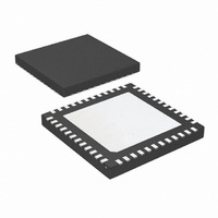
DS16EV5110ASQX/NOPB National Semiconductor, DS16EV5110ASQX/NOPB Datasheet - Page 8

DS16EV5110ASQX/NOPB
Manufacturer Part Number
DS16EV5110ASQX/NOPB
Description
IC EQUALIZER VIDEO 3D+C 48-LLP
Manufacturer
National Semiconductor
Type
Video Equalizerr
Datasheet
1.DS16EV5110ASQXNOPB.pdf
(20 pages)
Specifications of DS16EV5110ASQX/NOPB
Applications
HD Displays, DVI/HDMI
Mounting Type
Surface Mount
Package / Case
48-LLP
Lead Free Status / RoHS Status
Lead free / RoHS Compliant
Other names
DS16EV5110ASQX
www.national.com
System Management Bus (SMBus)
and Configuration Registers
The System Management Bus interface is compatible to SM-
Bus 2.0 physical layer specification. The use of the Chip
Select signal is required. Holding the CS pin High enables
the SMBus port allowing access to the configuration registers.
Holding the CS pin Low disables the device's SMBus allowing
communication from the host to other slave devices on the
bus. In the STANDBY state, the System Management Bus
remains active. When communication to other devices on the
SMBus is active, the CS signal for the DS16EV5110As must
be driven Low.
The address byte for all DS16EV5110As is AC'h. Based on
the SMBus 2.0 specification, the DS16EV5110A has a 7-bit
slave address of 1010110'b. The LSB is set to 0'b (for a
WRITE), thus the 8-bit value is 1010 1100 'b or AC'h.
The SDC and SDA pins are 3.3V LVCMOS signaling and in-
clude high-Z internal pull up resistors. External low
impedance pull up resistors maybe required depending upon
SMBus loading and speed. Note, these pins are not 5V tol-
erant.
Transfer of Data via the SMBus
During normal operation the data on SDA must be stable dur-
ing the time when SDC is High.
There are three unique states for the SMBus:
START: A High-to-Low transition on SDA while SDC is High
indicates a message START condition.
STOP: A Low-to-High transition on SDA while SDC is High
indicates a message STOP condition.
IDLE: If SDC and SDA are both High for a time exceeding
t
for a total exceeding the maximum specification for t
the bus will transfer to the IDLE state.
BUF
from the last detected STOP condition or if they are High
HIGH
then
8
SMBus Transactions
The device supports WRITE and READ transactions. See
Register Description table for register address, type (Read/
Write, Read Only), default value and function information.
Writing a Register
To write a register, the following protocol is used (see SMBus
2.0 specification).
1.
2.
3.
4.
5.
6.
7.
8.
9.
The WRITE transaction is completed, the bus goes IDLE and
communication with other SMBus devices may now occur.
Reading a Register
To read a register, the following protocol is used (see SMBus
2.0 specification).
1.
2.
3.
4.
5.
6.
7.
8.
9.
10. The Host drives a NACK bit “1”indicating end of the
11. The Host drives a STOP condition.
12. The Host de-selects the device by driving its SMBus CS
The READ transaction is completed, the bus goes IDLE and
communication with other SMBus devices may now occur.
Please see Table 1 for more information.
The Host (Master) selects the device by driving its
SMBus Chip Select (CS) signal High.
The Host drives a START condition, the 7-bit SMBus
address, and a “0” indicating a WRITE.
The Device (Slave) drives the ACK bit (“0”).
The Host drives the 8-bit Register Address.
The Device drives an ACK bit (“0”).
The Host drive the 8-bit data byte.
The Device drives an ACK bit (“0”).
The Host drives a STOP condition.
The Host de-selects the device by driving its SMBus CS
signal Low.
The Host (Master) selects the device by driving its
SMBus Chip Select (CS) signal High.
The Host drives a START condition, the 7-bit SMBus
address, and a “0” indicating a WRITE.
The Device (Slave) drives the ACK bit (“0”).
The Host drives the 8-bit Register Address.
The Device drives an ACK bit (“0”).
The Host drives a START condition.
The Host drives the 7-bit SMBus Address, and a “1”
indicating a READ.
The Device drives an ACK bit “0”.
The Device drives the 8-bit data value (register contents).
READ transfer.
signal Low.


