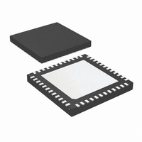
DS22EV5110SQX/NOPB National Semiconductor, DS22EV5110SQX/NOPB Datasheet - Page 2

DS22EV5110SQX/NOPB
Manufacturer Part Number
DS22EV5110SQX/NOPB
Description
IC EQUAL DVI HDMI RETIMER 48-LLP
Manufacturer
National Semiconductor
Type
Equalizerr
Datasheet
1.DS22EV5110SQENOPB.pdf
(18 pages)
Specifications of DS22EV5110SQX/NOPB
Applications
HDMI, DVI, Receivers
Mounting Type
Surface Mount
Package / Case
48-LLP
Lead Free Status / RoHS Status
Lead free / RoHS Compliant
Other names
DS22EV5110SQX
www.national.com
High Speed Differential I/O
C_IN−
C_IN+
D_IN0−
D_IN0+
D_IN1−
D_IN1+
D_IN2−
D_IN2+
C_OUT-
C_OUT+
D_OUT0−
D_OUT0+
D_OUT1–
D_OUT1+
D_OUT2−
D_OUT2+
Equalization Control
EQ2
EQ1
EQ0
De-Emphasis Control
DE1
DE0
Device Control
BYPASS
EN
SD
LOCK
VOD_CRL
LFp
LFn
Power
V
GND
Exposed
DAP
Pin Name
DD
Pin Descriptions
Pin Number
3, 6, 7,
10, 13,
22, 24,
27, 30,
15, 46
31, 34
DAP
11
12
36
35
33
32
29
28
26
25
37
38
39
42
43
47
44
45
14
48
40
41
1
2
4
5
8
9
O, LVCMOS Signal Detect Output pin.
O, LVCMOS Lock Indicator Output pin.
I, LVCMOS EQ2, EQ1 and EQ0 select the equalizer boost level for EQ channels. Internally pulled LOW
I, LVCMOS Enable Output Drivers. Internally pulled HIGH as default.
I/O, Type
LVCMOS
LVCMOS
O, CML
O, CML
O, CML
O, CML
Analog
Analog
I, CML
I, CML
I, CML
I, CML
Power
GND
GND
I,
I,
I,
I,
Inverting and non-inverting TMDS Clock inputs to the equalizer. An on-chip 50 Ω terminating
resistor connects C_IN+ to V
Inverting and non-inverting TMDS Data inputs to the equalizer. An on-chip 50 Ω terminating
resistor connects D_IN0+ to V
Inverting and non-inverting TMDS Data inputs to the equalizer. An on-chip 50 Ω terminating
resistor connects D_IN1+ to V
Inverting and non-inverting TMDS Data inputs to the equalizer. An on-chip 50 Ω terminating
resistor connects D_IN2+ to V
Inverting and non-inverting TMDS outputs from the equalizer. Open collector.
Inverting and non-inverting TMDS outputs from the equalizer. Open collector.
Inverting and non-inverting TMDS outputs from the equalizer. Open collector.
Inverting and non-inverting TMDS outputs from the equalizer. Open collector.
as default. See
DE1, DE0 select the DE-emphasis level for output drivers. Internally pulled low as default.
Refer to
Reclocker enable control. Internally pulled low as default.
H = Reclock and De-Emphasis function is bypassed.
L = Normal operation.
H = normal operation (enabled).
L = standby mode.
H = signal detected on all channels.
L = no signal detected on one or more channels.
H = PLL is locked.
L = PLL is not locked.
VOD control pin. Refer to
External resistance = 24 kΩ to GND, Output DC Coupled Application.
External resistance = 12 kΩ to GND, Output AC Coupled Application.
Loop filter capacitor pins.
See Functional Description.
V
A 0.1 µF bypass capacitor should be connected between each V
See Power Supply Bypassing for additional details.
Ground reference. GND should be tied to a solid ground plane through a low impedance
path.
Ground reference. The exposed pad at the center of the package must be connected to the
ground plane.
DD
= 3.3 V ±5%. V
Table
2.
Table
DD
1.
pins should be tied to the V
2
Table
DD
DD
DD
DD
and C_IN- to V
3. See Functional Description.
and D_IN0- to V
and D_IN1- to V
and D_IN2- to V
Description
DD
.
DD
DD
DD
DD
.
.
.
plane through a low inductance path.
DD
pin to the GND planes.


