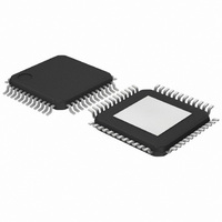
CX24109-11Z,518 NXP Semiconductors, CX24109-11Z,518 Datasheet - Page 15

CX24109-11Z,518
Manufacturer Part Number
CX24109-11Z,518
Description
IC SATELLITE TUNER DGTL 48-ETQFP
Manufacturer
NXP Semiconductors
Type
Tunerr
Datasheet
1.CX24109-11Z518.pdf
(40 pages)
Specifications of CX24109-11Z,518
Applications
Set-Top Boxes, Video Players
Mounting Type
Surface Mount
Package / Case
48-TQFP Exposed Pad, 48-eTQFP, 48-HTQFP, 48-VQFP
Lead Free Status / RoHS Status
Lead free / RoHS Compliant
Other names
548894
935287219518
935287219518
Available stocks
Company
Part Number
Manufacturer
Quantity
Price
Company:
Part Number:
CX24109-11Z,518
Manufacturer:
NXP Semiconductors
Quantity:
10 000
NXP Semiconductors
1.5
1.6
1.7
CX24109_N_1
Product data sheet
AGC and Control
Local Oscillator
Programming Interface
The L-band output from the LNB enters the IC through the RFIN pin and is immediately
amplified by the Voltage Controlled Attenuator block (VCA). The VCA functions as a variable
gain LNA. The noise figure and gain of the VCA are the dominant factors for the tuner’s noise
figure. The signal is then quadrature downconverted to I and Q baseband channels.
Additional amplifiers at baseband provide more variable gain for the AGC loop. Also at
baseband, variable low-pass filters provide anti-alias filtering and eliminate noise power from
adjacent carriers and spurious signals before they can impact the A/Ds in the demodulator
IC.
The AGC functionality for the CX24109 is split between the RF and baseband sections, and
provides 80 dB of variable gain. The primary control for the AGC is an analog voltage from
the demodulator IC. Programmable adjustments to the slope and offset of each variable gain
component in the tuner are available through the AGC control registers. Programming
information for the VGA and VCA is provided in
recommended default values for the programmable control bits versus symbol rate are listed
in
The local oscillator consists of a synthesizer and a VCO block, and is contained entirely
within the CX24109. The VCO block uses an innovative architecture that requires only a 5 V
source, eliminating the need for a 28 V power supply. It includes the required tank circuit.
The VCO block consists of a bank of eight oscillators operating at twice and four times the
input frequency with a continuous range from 2200 MHz to 4400 MHz. The VCOs overlap to
cover the frequency range from 950 MHz to 2150 MHz under all voltage, temperature, and
process variations. The VCO tuning range, combined with programmable ÷2 or ÷4 frequency
dividers, creates the continuous frequencies from 950 MHz to 2150 MHz for the local
oscillator. A simple tuning algorithm must be run by the host processor one time at power-up
to calibrate the VCO block. Conexant provides this program.
The synthesizer is also contained within the CX24109. It uses a 10.111 MHz reference
frequency and a reference divider, ÷R, to set the phase comparison frequency. Two
programming bits are used to configure the reference divider to divide by 10, 20, or 40, which
in turn sets the comparison frequency to 1.0111 MHz, 505 kHz, or 253 kHz, respectively. A
reference divider of 10 is recommended. The comparison frequency also determines the
frequency step size of the local oscillator. Another programmable divider is provided for the
VCO output. It consists of a 32/33 prescaler, a 9-bit N-counter (N-divider), a 5-bit A-counter
(A-divider), and a fixed ÷ 2 block. The programmable divider divides the VCO output from its
highest frequency to the minimum phase comparison frequency. The programmable charge
pump includes output currents of 1 mA, 2 mA, 3 mA, and 4 mA. Programming information for
the synthesizer can be found in
polarity, and referenced dividers are listed in
The typical loop filter bandwidth is set with external passive components and should be set
between 8 kHz and 15 kHz.
A three-wire serial interface with Clock, Data, and Enable lines is used to program the
CX24109. All digital signals are CMOS-compatible. The serial data carries the binary settings
for the programmable dividers, the VCO band select, the voltage-controlled attenuator, and
the voltage-controlled amplifiers. When the Enable line is low, data is shifted into an internal
shift register on the rising edge of the clock, and when the Enable line goes high, the stored
data is latched. The clock signal should be kept low when inactive. The maximum clock rate
is 1 MHz.
Table
8.
Figure 4
illustrates the relationship between the Clock, Data, and Enable signals.
Rev. 01 — 13 November 2008
Table
7. The recommended values for charge pump current,
Tables 9
Tables 4
Chapter 1: Functional Description
and 10.
and 5, respectively. The
CX24109
© NXP B.V. 2008. All rights reserved.
15


