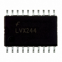
74LVX244M Fairchild Semiconductor, 74LVX244M Datasheet - Page 2

74LVX244M
Manufacturer Part Number
74LVX244M
Description
IC BUFF/DVR TRI-ST DUAL 20SOIC
Manufacturer
Fairchild Semiconductor
Series
74LVXr
Datasheet
1.74LVX244MTC.pdf
(6 pages)
Specifications of 74LVX244M
Logic Type
Buffer/Line Driver, Non-Inverting
Number Of Elements
2
Number Of Bits Per Element
4
Current - Output High, Low
4mA, 4mA
Voltage - Supply
2 V ~ 3.6 V
Operating Temperature
-40°C ~ 85°C
Mounting Type
Surface Mount
Package / Case
20-SOIC (7.5mm Width)
Logic Family
LVX
Number Of Channels Per Chip
8
Polarity
Non-Inverting
Supply Voltage (max)
3.6 V
Supply Voltage (min)
2 V
Maximum Operating Temperature
+ 85 C
Mounting Style
SMD/SMT
High Level Output Current
- 4 mA
Low Level Output Current
4 mA
Maximum Power Dissipation
180 mW
Minimum Operating Temperature
- 40 C
Number Of Lines (input / Output)
8 / 8
Output Type
3-State
Propagation Delay Time
14.9 ns at 2.7 V, 10.6 ns at 3.3 V
Logic Device Type
Buffer/Line Driver, Non Inverting
Supply Voltage Range
2V To 3.6V
Logic Case Style
SOIC
No. Of Pins
20
Operating Temperature Range
-40°C To +85°C
Filter Terminals
SMD
Rohs Compliant
Yes
Family Type
74LVX
Lead Free Status / RoHS Status
Lead free / RoHS Compliant
Available stocks
Company
Part Number
Manufacturer
Quantity
Price
Company:
Part Number:
74LVX244MSCX
Manufacturer:
NS
Quantity:
2 000
Part Number:
74LVX244MTCX
Manufacturer:
FAIRCHILD/仙童
Quantity:
20 000
www.fairchildsemi.com
V
V
V
V
I
I
I
V
V
V
V
OZ
IN
CC
Symbol
Symbol
Absolute Maximum Ratings
DC Electrical Characteristics
Noise Characteristics
Note 3: Input t
IH
IL
OH
OL
OLP
OLV
IHD
ILD
Supply Voltage (V
DC Input Diode Current (I
DC Input Voltage (V
DC Output Diode Current (I
DC Output Voltage (V
DC Output Source
DC V
Storage Temperature (T
Power Dissipation
V
V
V
or Sink Current (I
(I
CC
I
O
O
CC
or I
V
0.5V
HIGH Level Input
Voltage
LOW Level Input
Voltage
HIGH Level Output
Voltage
LOW Level Output
Voltage
3-STATE Output
Off-State Current
Input Leakage Current
Quiescent Supply Current
Quiet Output Maximum Dynamic V
Quiet Output Minimum Dynamic V
Minimum HIGH Level Dynamic Input Voltage
Maximum LOW Level Dynamic Input Voltage
or Ground Current
0.5V
CC
GND
r
t
f
)
0.5V
Parameter
3 ns
CC
O
I
)
)
)
O
)
STG
IK
)
OK
)
)
Parameter
V
2.0
3.0
3.6
2.0
3.0
3.6
2.0
3.0
3.0
2.0
3.0
3.0
3.6
3.6
3.6
CC
OL
(Note 3)
OL
0.5V to V
2.58
Min
65
1.5
2.0
2.4
1.9
2.9
0.5V to
(Note 1)
q
C to
0.5V to 7V
CC
T
180 mW
A
r
r
20 mA
20 mA
20 mA
25 mA
75 mA
150
Typ
2.0
3.0
0.0
0.0
7.0V
0.5V
25
q
q
C
C
2
r
Max
0.36
r
Recommended Operating
Conditions
Note 1: The “Absolute Maximum Ratings” are those values beyond which
the safety of the device cannot be guaranteed. The device should not be
operated at these limits. The parametric values defined in the Electrical
Characteristics tables are not guaranteed at the absolute maximum ratings.
The “Recommended Operating Conditions” table will define the conditions
for actual device operation.
Note 2: Unused inputs must be held HIGH or LOW. They may not float.
0.5
0.8
0.8
0.1
0.1
0.25
4.0
Supply Voltage (V
Input Voltage (V
Output Voltage (V
Operating Temperature (T
Input Rise and Fall Time (
0.1
V
(V)
3.3
3.3
3.3
3.3
CC
T
A
2.48
Min
1.5
2.0
2.4
1.9
2.9
40
q
Typ
C to
0.5
0.5
I
T
)
A
o
CC
Max
0.44
r
r
40.0
(Note 2)
0.5
0.8
0.8
0.1
0.1
)
2.5
1.0
85
)
25
q
C
q
Limit
C
0.8
2.0
0.8
0.8
'
A
Units
)
t/
P
P
P
'
V
V
V
V
A
A
A
V)
Units
V
V
V
V
V
V
V
V
V
V
IN
IN
IN
OUT
IN
IN
V
V
V
5.5V or GND
V
0 ns/V to 100 ns/V
IH
IH
IH
CC
V
Conditions
CC
or V
or V
or V
or GND
40
or GND
2.0V to 3.6V
IL
IL
IL
q
C
C to
0V to 5.5V
0V to V
L
I
I
I
I
I
I
50
50
50
50
OH
OH
OH
OL
OL
OL
(pF)
85
50
50
4 mA
50
50
4 mA
CC
q
P
P
C
A
A
P
P
A
A


