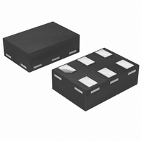
74LVC1G125GM,115 NXP Semiconductors, 74LVC1G125GM,115 Datasheet - Page 3

74LVC1G125GM,115
Manufacturer Part Number
74LVC1G125GM,115
Description
IC BUFF DVR TRI-ST N-INV 6XSON
Manufacturer
NXP Semiconductors
Series
74LVCr
Datasheet
1.74LVC1G125GV125.pdf
(19 pages)
Specifications of 74LVC1G125GM,115
Package / Case
6-XSON (Micropak™), SOT-886
Logic Type
Buffer/Line Driver, Non-Inverting
Number Of Elements
1
Number Of Bits Per Element
1
Current - Output High, Low
32mA, 32mA
Voltage - Supply
2 V ~ 5.5 V
Operating Temperature
-40°C ~ 125°C
Mounting Type
Surface Mount
Logic Family
74LVC
Number Of Channels Per Chip
1
Polarity
Non-Inverting
Supply Voltage (max)
5.5 V
Supply Voltage (min)
1.65 V
Maximum Operating Temperature
+ 125 C
Mounting Style
SMD/SMT
High Level Output Current
- 32 mA
Input Bias Current (max)
200 uA
Low Level Output Current
32 mA
Minimum Operating Temperature
- 40 C
Output Type
3-State
Propagation Delay Time
2.1 ns
Number Of Lines (input / Output)
1 / 1
Lead Free Status / RoHS Status
Lead free / RoHS Compliant
Lead Free Status / RoHS Status
Lead free / RoHS Compliant, Lead free / RoHS Compliant
Other names
568-4396-2
74LVC1G125GM-G
74LVC1G125GM-G
935277203115
74LVC1G125GM-G
74LVC1G125GM-G
935277203115
Available stocks
Company
Part Number
Manufacturer
Quantity
Price
Company:
Part Number:
74LVC1G125GM,115
Manufacturer:
NXP Semiconductors
Quantity:
4 000
NXP Semiconductors
6. Pinning information
Table 3.
7. Functional description
Table 4.
[1]
74LVC1G125
Product data sheet
Symbol
OE
A
GND
Y
n.c.
V
Input
OE
L
L
H
Fig 4.
CC
H = HIGH voltage level;
L = LOW voltage level;
X = don’t care;
Z = high-impedance OFF-state.
GND
OE
A
Pin configuration
SOT353-1 and SOT753
Pin description
Function table
1
2
3
74LVC1G125
6.1 Pinning
6.2 Pin description
Pin
SOT353-1, SOT753
1
2
3
4
-
5
001aaf198
[1]
5
4
V
Y
CC
A
L
H
X
All information provided in this document is subject to legal disclaimers.
Fig 5.
SOT886, SOT891, SOT1115, SOT1202
1
2
3
4
5
6
Rev. 9 — 29 December 2010
GND
OE
Pin configuration SOT886
A
Transparent top view
74LVC1G125
1
2
3
001aaf199
6
5
4
V
n.c.
Y
CC
Output
Y
L
H
Z
Fig 6.
ground (0 V)
data output
not connected
Description
output enable input
data input
supply voltage
Bus buffer/line driver; 3-state
GND
OE
Pin configuration SOT891,
SOT1115 and SOT1202
74LVC1G125
A
Transparent top view
74LVC1G125
1
2
3
© NXP B.V. 2010. All rights reserved.
001aaf400
6
5
4
V
n.c.
Y
CC
3 of 19


