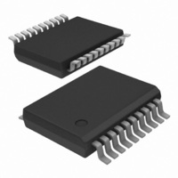
74ABT541DB,118 NXP Semiconductors, 74ABT541DB,118 Datasheet - Page 3

74ABT541DB,118
Manufacturer Part Number
74ABT541DB,118
Description
IC BUFF/DVR TRI-ST 8BIT 20SSOP
Manufacturer
NXP Semiconductors
Series
74ABTr
Datasheet
1.74ABT541DB118.pdf
(11 pages)
Specifications of 74ABT541DB,118
Package / Case
20-SSOP
Logic Type
Buffer/Line Driver, Non-Inverting
Number Of Elements
1
Number Of Bits Per Element
8
Current - Output High, Low
32mA, 64mA
Voltage - Supply
4.5 V ~ 5.5 V
Operating Temperature
-40°C ~ 85°C
Mounting Type
Surface Mount
Logic Family
ABT
Number Of Channels Per Chip
8
Polarity
Non-Inverting
Supply Voltage (max)
5.5 V
Supply Voltage (min)
4.5 V
Maximum Operating Temperature
+ 85 C
Mounting Style
SMD/SMT
High Level Output Current
- 32 mA
Input Bias Current (max)
30000 uA
Low Level Output Current
64 mA
Minimum Operating Temperature
- 40 C
Output Type
3-State
Propagation Delay Time
4.2 ns @ 5 V
Number Of Lines (input / Output)
8 / 8
Logical Function
Buffer/Line Driver
Number Of Elements
1
Number Of Channels
8
Number Of Inputs
8
Number Of Outputs
8
Operating Supply Voltage (typ)
5V
Package Type
SSOP
Operating Supply Voltage (max)
5.5V
Operating Supply Voltage (min)
4.5V
Quiescent Current
30mA
Technology
BiCMOS
Pin Count
20
Mounting
Surface Mount
Operating Temp Range
-40C to 85C
Operating Temperature Classification
Industrial
Lead Free Status / RoHS Status
Lead free / RoHS Compliant
Lead Free Status / RoHS Status
Lead free / RoHS Compliant, Lead free / RoHS Compliant
Other names
568-4540-2
74ABT541DB-T
74ABT541DB-T
935066500118
74ABT541DB-T
74ABT541DB-T
935066500118
1. Stresses beyond those listed may cause permanent damage to the device. These are stress ratings only and functional operation of the
2. The performance capability of a high-performance integrated circuit in conjunction with its thermal environment can create junction
3. The input and output voltage ratings may be exceeded if the input and output current ratings are observed.
Philips Semiconductors
LOGIC SYMBOL (IEEE/IEC)
ABSOLUTE MAXIMUM RATINGS
NOTES:
1998 Jan 16
SYMBOL
Octal buffer/line driver (3-State)
device at these or any other conditions beyond those indicated under “recommended operating conditions” is not implied. Exposure to
absolute-maximum-rated conditions for extended periods may affect device reliability.
temperatures which are detrimental to reliability. The maximum junction temperature of this integrated circuit should not exceed 150 C.
V
I
V
T
I
OUT
I
OUT
V
OK
CC
IK
stg
I
DC supply voltage
DC input diode current
DC input voltage
DC output diode current
DC output voltage
DC output current
Storage temperature range
19
1
2
3
4
5
6
7
8
9
&
PARAMETER
3
EN
3
SA00204
1, 2
18
17
16
15
14
13
12
11
output in Off or High state
3
output in Low state
CONDITIONS
PIN DESCRIPTION
FUNCTION TABLE
H = High voltage level
L = Low voltage level
X = Don’t care
Z = High impedance ”off” state
PIN NUMBER
18, 17, 16, 15,
V
14, 13, 12, 11
OE0
V
O
X
H
L
L
I
2, 3, 4, 5,
6, 7, 8, 9
< 0
< 0
1, 19
10
20
INPUTS
OE1
H
L
L
X
OE0, OE1
SYMBOL
A0 – A7
Y0 – Y7
An
H
X
X
L
GND
V
CC
OUTPUTS
–0.5 to +7.0
–1.2 to +7.0
–0.5 to +5.5
–65 to 150
RATING
Yn
Data inputs
Data outputs
Output enables
Ground (0V)
Positive supply voltage
H
L
Z
Z
–18
–50
128
NAME AND FUNCTION
74ABT541
Product specification
UNIT
mA
mA
mA
V
V
V
C


