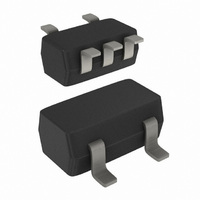
74HCT1G125GW,125 NXP Semiconductors, 74HCT1G125GW,125 Datasheet - Page 9

74HCT1G125GW,125
Manufacturer Part Number
74HCT1G125GW,125
Description
IC BUS BUFF DVR TRI-ST 5TSSOP
Manufacturer
NXP Semiconductors
Series
74HCTr
Datasheet
1.74HC1G125GW125.pdf
(16 pages)
Specifications of 74HCT1G125GW,125
Package / Case
SC-70-5, SC-88A, SOT-323-5, SOT-353, 5-TSSOP
Logic Type
Buffer/Line Driver, Non-Inverting
Number Of Elements
1
Number Of Bits Per Element
1
Current - Output High, Low
6mA, 6mA
Voltage - Supply
4.5 V ~ 5.5 V
Operating Temperature
-40°C ~ 125°C
Mounting Type
Surface Mount
Logic Family
HCT
Number Of Channels Per Chip
1
Polarity
Non-Inverting
Supply Voltage (max)
5.5 V
Supply Voltage (min)
4.5 V
Maximum Operating Temperature
+ 125 C
Mounting Style
SMD/SMT
High Level Output Current
- 6 mA
Input Bias Current (max)
20 uA
Low Level Output Current
6 mA
Minimum Operating Temperature
- 40 C
Output Type
3-State
Propagation Delay Time
11 ns (Typ) @ 4.5 V
Number Of Lines (input / Output)
1 / 1
Lead Free Status / RoHS Status
Lead free / RoHS Compliant
Lead Free Status / RoHS Status
Lead free / RoHS Compliant, Lead free / RoHS Compliant
Other names
568-4582-2
74HCT1G125GW-G
74HCT1G125GW-G
935245680125
74HCT1G125GW-G
74HCT1G125GW-G
935245680125
Philips Semiconductors
74HC_HCT1G125_5
Product data sheet
Table 11:
Voltages are referenced to GND (ground = 0 V); CL = 50 pF unless otherwise specified; for test
circuit see
[1]
[2]
Symbol Parameter
T
t
t
t
t
t
t
C
T
t
t
t
t
t
t
PHL
PLH
PZH
PZL
PHZ
PLZ
PHL
PLH
PZH
PZL
PHZ
PLZ
amb
amb
PD
,
,
,
,
,
,
All typical values are measured at T
C
P
f
f
C
V
N = number of inputs switching;
i
o
(C
D
CC
= 40 C to +85 C
= 40 C to +125 C
PD
= input frequency in MHz;
L
= output frequency in MHz;
= output load capacitance in pF;
= C
L
is used to determine the dynamic power dissipation (P
= supply voltage in V;
propagation delay A to Y
3-state output enable time
OE to Y
3-state output disable time
OE to Y
power dissipation
capacitance
propagation delay A to Y
3-state output enable time
OE to Y
3-state output disable time
OE to Y
PD
Figure 8
V
Dynamic characteristics 74HCT1G125
CC
2
V
CC
f
o
2
) = sum of the outputs.
f
i
Rev. 05 — 23 December 2005
N + (C
[1]
L
V
CC
amb
74HC1G125; 74HCT1G125
2
= 25 C.
Conditions
see
V
V
V
V
V
V
f
I
CC
CC
CC
CC
CC
o
V
V
= GND to V
) where:
CC
CC
Figure 6
= 4.5 V; see
= 4.5 V; see
= 4.5 V; see
= 4.5 V; see
= 4.5 V; see
= 4.5 V
= 5 V; C
CC
L
D
= 15 pF
Figure 7
Figure 7
Figure 6
Figure 7
Figure 7
1.5 V
in W).
Bus buffer/line driver; 3-state
© Koninklijke Philips Electronics N.V. 2005. All rights reserved.
[2]
Min
-
-
-
-
-
-
-
-
Typ
11
10
10
11
27
-
-
-
Max Unit
30
-
35
31
-
36
42
38
ns
ns
ns
ns
pF
ns
ns
ns
9 of 16


