HEF40244BP,652 NXP Semiconductors, HEF40244BP,652 Datasheet - Page 2
HEF40244BP,652
Manufacturer Part Number
HEF40244BP,652
Description
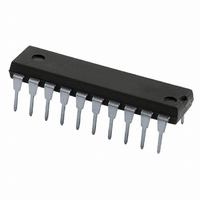
IC BUFF/DVR TRI-ST DUAL 20DIP
Manufacturer
NXP Semiconductors
Series
4000Br
Specifications of HEF40244BP,652
Logic Type
Buffer/Line Driver, Non-Inverting
Number Of Elements
2
Number Of Bits Per Element
4
Current - Output High, Low
62mA, 45mA
Voltage - Supply
4.5 V ~ 15.5 V
Operating Temperature
-40°C ~ 85°C
Mounting Type
Through Hole
Package / Case
20-DIP (0.300", 7.62mm)
Logic Family
HEF4000
Number Of Channels Per Chip
8
Polarity
Non-Inverting
Supply Voltage (max)
15 V
Supply Voltage (min)
3 V
Maximum Operating Temperature
+ 85 C
Mounting Style
Through Hole
High Level Output Current
- 19.5 mA
Low Level Output Current
30 mA
Minimum Operating Temperature
- 40 C
Number Of Lines (input / Output)
8 / 8
Output Type
3-State
Propagation Delay Time
190 ns at 5 V, 80 ns at 10 V, 60 ns at 15 V
Lead Free Status / RoHS Status
Lead free / RoHS Compliant
Other names
568-3089-5
933567170652
HEF40244BPN
933567170652
HEF40244BPN


Philips Semiconductors
DESCRIPTION
The HEF40244B is an octal non-inverting buffer with
3-state outputs. It features output stages with high current
output capability suitable for driving highly capacitive
loads.
The 3-state outputs are controlled by the output enable
inputs EO
assume a high impedance OFF-state. The device also
features hysteresis on all inputs to improve noise
immunity.
Schmitt-trigger action in the inputs makes the circuit highly
tolerant to slower input rise and fall times.
The HEF40244B is pin and functionally compatible with
the TTL ‘244’ device.
January 1995
Octal buffers with 3-state outputs
A
and EO
Fig.1 Functional diagram.
B
. A HIGH on EO causes the outputs to
2
PINNING
FAMILY DATA, I
See Family Specifications
HEF40244BP(N): 20-lead DIL; plastic (SOT146-1)
HEF40244BD(F): 20-lead DIL; ceramic (cerdip) (SOT152)
HEF40244BT(D): 20-lead SO; plastic (SOT163-1)
( ): Package Designator North America
I
I
O
O
EO
A1
B1
A1
B1
A
to I
to I
to O
to O
, EO
A4
B4
A4
B4
B
DD
Fig.2 Pinning diagram.
inputs
inputs
bus outputs
bus outputs
output enable inputs (active LOW)
LIMITS category buffers
Product specification
HEF40244B
buffers
Related parts for HEF40244BP,652
Image
Part Number
Description
Manufacturer
Datasheet
Request
R

Part Number:
Description:
Octal Buffers With 3-state Outputs
Manufacturer:
NXP Semiconductors
Datasheet:
Part Number:
Description:
NXP Semiconductors designed the LPC2420/2460 microcontroller around a 16-bit/32-bitARM7TDMI-S CPU core with real-time debug interfaces that include both JTAG andembedded trace
Manufacturer:
NXP Semiconductors
Datasheet:

Part Number:
Description:
NXP Semiconductors designed the LPC2458 microcontroller around a 16-bit/32-bitARM7TDMI-S CPU core with real-time debug interfaces that include both JTAG andembedded trace
Manufacturer:
NXP Semiconductors
Datasheet:
Part Number:
Description:
NXP Semiconductors designed the LPC2468 microcontroller around a 16-bit/32-bitARM7TDMI-S CPU core with real-time debug interfaces that include both JTAG andembedded trace
Manufacturer:
NXP Semiconductors
Datasheet:
Part Number:
Description:
NXP Semiconductors designed the LPC2470 microcontroller, powered by theARM7TDMI-S core, to be a highly integrated microcontroller for a wide range ofapplications that require advanced communications and high quality graphic displays
Manufacturer:
NXP Semiconductors
Datasheet:
Part Number:
Description:
NXP Semiconductors designed the LPC2478 microcontroller, powered by theARM7TDMI-S core, to be a highly integrated microcontroller for a wide range ofapplications that require advanced communications and high quality graphic displays
Manufacturer:
NXP Semiconductors
Datasheet:
Part Number:
Description:
The Philips Semiconductors XA (eXtended Architecture) family of 16-bit single-chip microcontrollers is powerful enough to easily handle the requirements of high performance embedded applications, yet inexpensive enough to compete in the market for hi
Manufacturer:
NXP Semiconductors
Datasheet:
Part Number:
Description:
The XA-S3 device is a member of Philips Semiconductors? XA(eXtended Architecture) family of high performance 16-bitsingle-chip microcontrollers
Manufacturer:
NXP Semiconductors
Datasheet:

Part Number:
Description:
The NXP BlueStreak LH75401/LH75411 family consists of two low-cost 16/32-bit System-on-Chip (SoC) devices
Manufacturer:
NXP Semiconductors
Datasheet:
Part Number:
Description:
The NXP LPC3130/3131 combine an 180 MHz ARM926EJ-S CPU core, high-speed USB2
Manufacturer:
NXP Semiconductors
Datasheet:
Part Number:
Description:
The NXP LPC3141 combine a 270 MHz ARM926EJ-S CPU core, High-speed USB 2
Manufacturer:
NXP Semiconductors
Part Number:
Description:
The NXP LPC3143 combine a 270 MHz ARM926EJ-S CPU core, High-speed USB 2
Manufacturer:
NXP Semiconductors

Part Number:
Description:
The NXP LPC3152 combines an 180 MHz ARM926EJ-S CPU core, High-speed USB 2
Manufacturer:
NXP Semiconductors
Part Number:
Description:
The NXP LPC3154 combines an 180 MHz ARM926EJ-S CPU core, High-speed USB 2
Manufacturer:
NXP Semiconductors