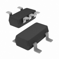
74LVC1G17GV,125 NXP Semiconductors, 74LVC1G17GV,125 Datasheet - Page 8

74LVC1G17GV,125
Manufacturer Part Number
74LVC1G17GV,125
Description
IC BUFFER SCHMITT TRIGGER SC74A
Manufacturer
NXP Semiconductors
Series
74LVCr
Datasheet
1.74LVC1G17GM115.pdf
(19 pages)
Specifications of 74LVC1G17GV,125
Package / Case
SC-74-5, SOT-753
Logic Type
Schmitt Trigger - Buffer, Driver
Number Of Elements
1
Number Of Bits Per Element
1
Current - Output High, Low
32mA, 32mA
Voltage - Supply
2 V ~ 5.5 V
Operating Temperature
-40°C ~ 125°C
Mounting Type
Surface Mount
Logic Family
LVC
Number Of Channels Per Chip
1
Polarity
Non-Inverting
Supply Voltage (max)
5.5 V
Supply Voltage (min)
1.65 V
Maximum Operating Temperature
+ 125 C
Mounting Style
SMD/SMT
High Level Output Current
- 32 mA
Input Bias Current (max)
200 uA
Low Level Output Current
32 mA
Minimum Operating Temperature
- 40 C
Propagation Delay Time
3.2 ns (Typ) @ 2.7 V or 3 ns (Typ) @ 3.3 V or 2.2 ns (Typ) @ 5 V
Number Of Lines (input / Output)
1 / 1
Lead Free Status / RoHS Status
Lead free / RoHS Compliant
Lead Free Status / RoHS Status
Lead free / RoHS Compliant, Lead free / RoHS Compliant
Other names
74LVC1G17GV-G
74LVC1G17GV-G
935270081125
74LVC1G17GV-G
935270081125
NXP Semiconductors
12. Waveforms
Table 10.
74LVC1G17
Product data sheet
Supply voltage
V
1.65 V to 1.95 V
2.3 V to 2.7 V
2.7 V
3.0 V to 3.6 V
4.5 V to 5.5 V
Fig 10. The input A to output Y propagation delay times
Fig 11. Test circuit for measuring switching times
CC
Measurement points are given in
V
Test data is given in
Definitions for test circuit:
R
C
R
V
OL
L
L
T
EXT
Measurement points
= Load resistance.
= Load capacitance including jig and probe capacitance.
= Termination resistance should be equal to the output impedance Z
and V
= External voltage for measuring switching times.
OH
are typical output voltage levels that occur with the output load.
Table
11.
Y output
A input
Table
Input
V
0.5 × V
0.5 × V
1.5 V
1.5 V
0.5 × V
G
All information provided in this document is subject to legal disclaimers.
M
GND
10.
V
V
OH
OL
V
V
I
Rev. 7 — 10 November 2010
CC
CC
CC
I
R T
V
M
DUT
V
CC
V
M
t
PHL
V
O
C L
o
of the pulse generator.
V
mna616
EXT
R L
R L
mnb153
t
Output
V
0.5 × V
0.5 × V
1.5 V
1.5 V
0.5 × V
PLH
M
Single Schmitt trigger buffer
CC
CC
CC
74LVC1G17
© NXP B.V. 2010. All rights reserved.
8 of 19


