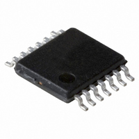
74LVC07APW,118 NXP Semiconductors, 74LVC07APW,118 Datasheet - Page 9

74LVC07APW,118
Manufacturer Part Number
74LVC07APW,118
Description
IC BUFF HEX OPEN DRAIN 14TSSOP
Manufacturer
NXP Semiconductors
Series
74LVCr
Datasheet
1.74LVC07ABQ115.pdf
(14 pages)
Specifications of 74LVC07APW,118
Logic Type
Buffer/Line Driver, Non-Inverting with Open Drain
Package / Case
14-TSSOP
Number Of Elements
6
Number Of Bits Per Element
1
Current - Output High, Low
32mA, 32mA
Voltage - Supply
2 V ~ 5.5 V
Operating Temperature
-40°C ~ 125°C
Mounting Type
Surface Mount
Logic Family
74LVC
Number Of Channels Per Chip
6
Polarity
Non-Inverting
Supply Voltage (max)
5.5 V
Supply Voltage (min)
1.65 V
Maximum Operating Temperature
125 C
Mounting Style
SMD/SMT
Input Bias Current (max)
10 uA
Low Level Output Current
32 mA
Maximum Power Dissipation
500 mW
Minimum Operating Temperature
- 40 C
Number Of Lines (input / Output)
6 / 6
Output Type
Open Drain
Propagation Delay Time
2.5 ns
Logical Function
Buffer/Driver
Number Of Elements
6
Number Of Channels
6
Number Of Inputs
6
Number Of Outputs
6
Operating Supply Voltage (typ)
1.8/2.5/3.3/5V
Package Type
TSSOP
High Level Output Current
32mA
Operating Supply Voltage (max)
5.5V
Operating Supply Voltage (min)
1.65V
Quiescent Current
10uA
Technology
CMOS
Pin Count
14
Mounting
Surface Mount
Operating Temp Range
-40C to 125C
Operating Temperature Classification
Automotive
Lead Free Status / RoHS Status
Lead free / RoHS Compliant
Lead Free Status / RoHS Status
Lead free / RoHS Compliant, Lead free / RoHS Compliant
Other names
568-2286-2
74LVC07APW-T
935265482118
74LVC07APW-T
935265482118
Philips Semiconductors
AC WAVEFORMS
2003 Nov 11
handbook, full pagewidth
handbook, full pagewidth
Hex buffer with open-drain outputs
Definitions for test circuits:
R
C
R
<2.7 V
1.65 to 1.95 V
2.3 to 2.7 V
2.7 V
3.0 to 3.6 V
4.5 to 5.5 V
L
L
T
2.7 to 3.6 V
4.5 to 5.5 V
= Load resistor.
= Load capacitance including jig and probe capacitance.
= Termination resistance should be equal to the output impedance Z
V
CC
V
CC
0.5
1.5 V
0.5
2
2
6 V
6 V
2
V
V
V
V
CC
CC
V
V
V
M
ext
CC
CC
CC
nA input
nY output
Fig.6 The input nA to output nY propagation delays.
MNA530
GENERATOR
GND
V CC
V
V
2.7 V
2.7 V
V
V OL
V
V
V
CC
CC
CC
V I
OL
OL
OL
PULSE
Fig.7 Load circuitry for switching times.
V
+ 0.15 V
+ 0.3 V
+ 0.3 V
I
V
X
V M
t PLZ
30 pF
30 pF
50 pF
50 pF
50 pF
V I
C
L
o
R T
V X
of the pulse generator.
9
D.U.T.
V CC
1 k
500
500
500
500
R
V O
L
t PZL
C L
V ext
R L
R L
V M
MNA528
Product specification
74LVC07A


