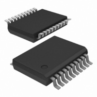
74LVC241ADB,118 NXP Semiconductors, 74LVC241ADB,118 Datasheet - Page 2

74LVC241ADB,118
Manufacturer Part Number
74LVC241ADB,118
Description
IC BUFF/DVR TRI-ST DUAL 20SSOP
Manufacturer
NXP Semiconductors
Series
74LVCr
Datasheet
1.74LVC241APW118.pdf
(10 pages)
Specifications of 74LVC241ADB,118
Logic Type
Buffer/Line Driver, Non-Inverting
Number Of Elements
2
Number Of Bits Per Element
4
Current - Output High, Low
24mA, 24mA
Voltage - Supply
1.2 V ~ 3.6 V
Operating Temperature
-40°C ~ 85°C
Mounting Type
Surface Mount
Package / Case
20-SSOP
Lead Free Status / RoHS Status
Lead free / RoHS Compliant
Other names
74LVC241ADB-T
74LVC241ADB-T
935213500118
74LVC241ADB-T
935213500118
Philips Semiconductors
FEATURES
QUICK REFERENCE DATA
GND = 0 V; T
ORDERING INFORMATION
PIN CONFIGURATION
t
C
C
20-Pin Plastic SO
20-Pin Plastic SSOP Type II
20-Pin Plastic TSSOP Type I
1998 May 20
PHL
SYMBOL
5-Volt tolerant inputs/outputs, for interfacing with 5-volt logic.
Supply voltage range of 1.2 to 3.6 V
In accordance with JEDEC standard no. 8-1A
CMOS lower power consumption
Direct interface with TTL levels
High impedance when V
Octal buffer/line driver with 5-volt tolerant
inputs/outputs (3-State)
I
PD
/t
PLH
PACKAGES
amb
Propagation delay
1A
2A
Input capacitance
Power dissipation capacitance per buffer
n
n
= 25 C; t
to 1Y
to 2Y
GND
1OE
1A
2Y
1A
2Y
1A
2Y
1A
2Y
0
0
1
1
2
2
3
3
n
n
;
10
2
3
4
5
6
7
8
9
1
r
CC
= t
PARAMETER
= 0 V
f
2.5 ns
TEMPERATURE RANGE
SV00614
19
15
14
12
20
18
17
16
13
11
–40 C to +85 C
–40 C to +85 C
–40 C to +85 C
V
2OE
1Y
2A
1Y
2A
1Y
2A
1Y
2A
CC
0
0
1
1
2
2
3
3
C
V
V
L
CC
CC
= 50 pF;
OUTSIDE NORTH AMERICA
= 3.3 V
= 3.3 V
2
CONDITIONS
74LVC241A PW
74LVC241A DB
74LVC241A D
DESCRIPTION
The 74LVC241A is a high-performance, low-power, low-voltage,
Si-gate CMOS device and superior to most advanced CMOS
compatible TTL families.
Inputs can be driven from either 3.3 V or 5 V devices. In 3-State
operation, outputs can handle 5 V. This feature allows the use of
these devices as translators in a mixed 3.3 V/5 V environment.
The 74LVC241A is an octal non-inverting buffer/line driver with 3-State
outputs. The 3-State outputs are controlled by the output enable inputs
1OE and 2OE. Schmitt-trigger action at all inputs makes the circuit
highly tolerant for slower input rise and fall times.
PIN DESCRIPTION
1
2, 4, 6, 8
3, 5, 7, 9
10
17, 15, 13, 11
18, 16, 14, 12
19
20
NUMBER
PIN
1OE
1A
2Y
GND
2A
1Y
2OE
V
SYMBOL
CC
0
0
0
0
to 2A
to 1Y
to 1A
to 2Y
NORTH AMERICA
7LVC241APW DH
3
3
3
3
74LVC241A DB
74LVC241A D
Output enable input (active LOW)
Data inputs
Bus outputs
Ground (0 V)
Data inputs
Bus outputs
Output enable input (active HIGH)
Positive supply voltage
TYPICAL
3.2
5.0
25
FUNCTION
74LVC241A
Product specification
853-2005 19419
PKG. DWG. #
SOT163-1
SOT339-1
SOT360-1
UNIT
pF
pF
ns


