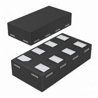
74LVC3G17GT,115 NXP Semiconductors, 74LVC3G17GT,115 Datasheet - Page 8

74LVC3G17GT,115
Manufacturer Part Number
74LVC3G17GT,115
Description
IC BUFF SCHMT TRG TRPL 8XSON
Manufacturer
NXP Semiconductors
Series
74LVCr
Datasheet
1.74LVC3G17DP125.pdf
(23 pages)
Specifications of 74LVC3G17GT,115
Package / Case
8-XSON
Logic Type
Schmitt Trigger - Buffer, Driver
Number Of Elements
3
Number Of Bits Per Element
1
Current - Output High, Low
32mA, 32mA
Voltage - Supply
2 V ~ 5.5 V
Operating Temperature
-40°C ~ 125°C
Mounting Type
Surface Mount
Logic Family
LVC
Number Of Channels Per Chip
3
Polarity
Non-Inverting
Supply Voltage (max)
5.5 V
Supply Voltage (min)
1.65 V
Maximum Operating Temperature
+ 125 C
Mounting Style
SMD/SMT
High Level Output Current
- 32 mA
Input Bias Current (max)
40 uA
Low Level Output Current
32 mA
Minimum Operating Temperature
- 40 C
Propagation Delay Time
3.8 ns (Typ) @ 2.7 V or 3.6 ns (Typ) @ 3.3 V or 2.7 ns (Typ) @ 5 V
Number Of Lines (input / Output)
3 / 3
Lead Free Status / RoHS Status
Lead free / RoHS Compliant
Lead Free Status / RoHS Status
Lead free / RoHS Compliant, Lead free / RoHS Compliant
Other names
74LVC3G17GT-G
74LVC3G17GT-G
935278935115
74LVC3G17GT-G
935278935115
NXP Semiconductors
13. Waveforms
Table 9.
74LVC3G17
Product data sheet
Supply voltage
V
1.65 V to 1.95 V
2.3 V to 2.7 V
2.7 V
3.0 V to 3.6 V
4.5 V to 5.5 V
Fig 8.
CC
Measurement points are given in
V
The input (nA) to output (nY) propagation delays and the output transition times
OL
Measurement points
and V
OH
are typical output voltage drops that occur with the output load.
nA input
nY output
Table
All information provided in this document is subject to legal disclaimers.
Input
V
0.5 × V
0.5 × V
1.5 V
1.5 V
0.5 × V
GND
M
V
V
9.
OH
OL
V
I
Rev. 7 — 4 November 2010
CC
CC
CC
t
PLH
Triple non-inverting Schmitt trigger with 5 V tolerant input
V
M
V
M
V
M
V
M
t
mnb072
PHL
Output
V
0.5 × V
0.5 × V
1.5 V
1.5 V
0.5 × V
M
CC
CC
CC
74LVC3G17
© NXP B.V. 2010. All rights reserved.
8 of 23


