74ALVT162244DL,118 NXP Semiconductors, 74ALVT162244DL,118 Datasheet - Page 6
74ALVT162244DL,118
Manufacturer Part Number
74ALVT162244DL,118
Description
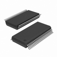
IC BUFF DVR TRI-ST 16BIT 48SSOP
Manufacturer
NXP Semiconductors
Series
74ALVTr
Datasheet
1.74ALVT162244DGG51.pdf
(10 pages)
Specifications of 74ALVT162244DL,118
Package / Case
48-SSOP
Logic Type
Buffer/Line Driver, Non-Inverting
Number Of Elements
4
Number Of Bits Per Element
4
Current - Output High, Low
8mA, 12mA; 12mA, 12mA
Voltage - Supply
2.3 V ~ 2.7 V, 3 V ~ 3.6 V
Operating Temperature
-40°C ~ 85°C
Mounting Type
Surface Mount
Logic Family
ALVT
Number Of Channels Per Chip
16
Polarity
Non-Inverting
Supply Voltage (max)
3.6 V
Supply Voltage (min)
2.3 V
Maximum Operating Temperature
+ 85 C
Mounting Style
SMD/SMT
High Level Output Current
- 12 mA
Input Bias Current (max)
5000 uA
Low Level Output Current
12 mA
Minimum Operating Temperature
- 40 C
Output Type
3-State
Propagation Delay Time
2.7 ns (Typ) @ 2.5 V or 2.2 ns (Typ) @ 3.3 V
Number Of Lines (input / Output)
16 / 16
Lead Free Status / RoHS Status
Lead free / RoHS Compliant
Lead Free Status / RoHS Status
Lead free / RoHS Compliant, Lead free / RoHS Compliant
Other names
74ALVT162244DL-T
74ALVT162244DL-T
935209500118
74ALVT162244DL-T
935209500118


1. All typical values are at V
2. This is the increase in supply current for each input at the specified voltage level other than V
3. This parameter is valid for any V
4. Unused pins at V
5. I
6. Not guaranteed.
1. All typical values are at V
Philips Semiconductors
DC ELECTRICAL CHARACTERISTICS (2.5V "0.2V RANGE)
NOTES:
AC CHARACTERISTICS (2.5V "0.2V RANGE)
GND = 0V; t
NOTE:
1998 Oct 07
SYMBOL
2.5V/3.3V 16-bit buffer/driver with
30 termination resistors (3-State)
I
transition time of 100 sec is permitted. This parameter is valid for T
I
I
SYMBOL
PU/PD
HOLD
HOLD
I
I
CCZ
V
I
I
I
I
V
V
OFF
I
OZH
CCH
CCL
CCZ
OZL
EX
I
OH
OL
I
I
CC
t
t
IK
t
t
t
t
I
I
PLH
PHL
PZH
PHZ
PZL
PLZ
is measured with outputs pulled up to V
R
Input clamp voltage
High-level output voltage
Low-level output voltage
Input leakage current
In ut leakage current
Off current
Bus Hold current
Data inputs
Current into an output in the
High state when V
Power up/down 3-State output
current
3-State output High current
3-State output Low current
Quiescent supply current
Additional supply current per
input pin
= t
F
= 2.5ns; C
Propagation delay
nAx to nBx or nBx to nAx
Output enable time
to High and Low level
Output disable time
from High and Low Level
CC
3
2
PARAMETER
or GND.
6
CC
CC
L
= 50pF; R
= 2.5V and T
= 2.5V and T
O
PARAMETER
> V
CC
CC
between 0V and 1.2V with a transition time of up to 10msec. From V
L
= 500 ; T
amb
amb
CC
V
V
V
V
V
V
V
V
V
V
V
V
OE/OE = Don’t care
V
V
V
V
V
V
Other inputs at V
= 25 C.
= 25 C.
CC
CC
CC
CC
CC
CC
CC
CC
CC
CC
O
CC
CC
CC
CC
CC
CC
CC
or pulled down to ground.
= 5.5V; V
amb
= 2.3V; I
= 2.3V; I
= 2.3V; I
= 2.7V; V
= 0 or 2.7V; V
= 2.7V; V
= 2.7V; V
= 0V; V
= 2.3V; V
= 2.3V; V
= 2.7V; V
= 2.7V; V
= 2.7V; Outputs High, V
= 2.7V; Outputs Low, V
= 2.7V; Outputs Disabled; V
= 2.3V to 2.7V; One input at V
1.2V; V
= –40 C to +85 C.
I
CC
IK
OH
OL
or V
O
I
I
I
I
I
O
O
= V
= V
= 0
= 0.7V
= 1.7V
= –18mA
= 0.5V to V
= 2.3V
= 2.3V; V
= 0.5V; V
= 12mA
= –8mA
CC
O
TEST CONDITIONS
I
CC
CC
= 0 to 4.5V
= 5.5V
or GND
WAVEFORM
or GND
6
amb
I
I
= V
= V
CC
I
= 25 C only.
1
2
2
I
= GND or V
= GND or V
; V
IL
IL
or V
or V
I
I
= GND or V
= GND or V
CC
IH
IH
–0.6V,
CC,
CC,
Control pins
Data pins
Data ins
I
I
O
CC
CC,
O
MIN
= 0
1.5
1.5
2.0
2.0
1.0
1.0
= 0
;
CC
I
O
or GND
= 0
V
4
4
CC
5
= 2.5V "0.2V
LIMITS
TYP
CC
Temp = -40 C to +85 C
2.7
2.3
4.4
3.0
2.8
2.0
MIN
1.7
= 1.2V to V
1
74ALVT162244
LIMITS
–0.85
TYP
0.04
0.04
0.04
115
–10
0.6
0.1
0.1
0.1
0.1
0.1
0.5
0.5
2.5
10
MAX
1
4.2
3.7
6.8
5.1
4.6
3.3
CC
1
Product specification
= 2.5V
MAX
–1.2
125
0.7
0.1
4.5
0.1
0.4
10
100
100
–5
-5
1
5
1
UNIT
0.2V a
ns
ns
ns
UNIT
mA
mA
V
V
V
A
A
A
A
A
A
A
A
A
Related parts for 74ALVT162244DL,118
Image
Part Number
Description
Manufacturer
Datasheet
Request
R

Part Number:
Description:
NXP Semiconductors designed the LPC2420/2460 microcontroller around a 16-bit/32-bitARM7TDMI-S CPU core with real-time debug interfaces that include both JTAG andembedded trace
Manufacturer:
NXP Semiconductors
Datasheet:

Part Number:
Description:
NXP Semiconductors designed the LPC2458 microcontroller around a 16-bit/32-bitARM7TDMI-S CPU core with real-time debug interfaces that include both JTAG andembedded trace
Manufacturer:
NXP Semiconductors
Datasheet:
Part Number:
Description:
NXP Semiconductors designed the LPC2468 microcontroller around a 16-bit/32-bitARM7TDMI-S CPU core with real-time debug interfaces that include both JTAG andembedded trace
Manufacturer:
NXP Semiconductors
Datasheet:
Part Number:
Description:
NXP Semiconductors designed the LPC2470 microcontroller, powered by theARM7TDMI-S core, to be a highly integrated microcontroller for a wide range ofapplications that require advanced communications and high quality graphic displays
Manufacturer:
NXP Semiconductors
Datasheet:
Part Number:
Description:
NXP Semiconductors designed the LPC2478 microcontroller, powered by theARM7TDMI-S core, to be a highly integrated microcontroller for a wide range ofapplications that require advanced communications and high quality graphic displays
Manufacturer:
NXP Semiconductors
Datasheet:
Part Number:
Description:
The Philips Semiconductors XA (eXtended Architecture) family of 16-bit single-chip microcontrollers is powerful enough to easily handle the requirements of high performance embedded applications, yet inexpensive enough to compete in the market for hi
Manufacturer:
NXP Semiconductors
Datasheet:
Part Number:
Description:
The XA-S3 device is a member of Philips Semiconductors? XA(eXtended Architecture) family of high performance 16-bitsingle-chip microcontrollers
Manufacturer:
NXP Semiconductors
Datasheet:

Part Number:
Description:
The NXP BlueStreak LH75401/LH75411 family consists of two low-cost 16/32-bit System-on-Chip (SoC) devices
Manufacturer:
NXP Semiconductors
Datasheet:
Part Number:
Description:
The NXP LPC3130/3131 combine an 180 MHz ARM926EJ-S CPU core, high-speed USB2
Manufacturer:
NXP Semiconductors
Datasheet:
Part Number:
Description:
The NXP LPC3141 combine a 270 MHz ARM926EJ-S CPU core, High-speed USB 2
Manufacturer:
NXP Semiconductors
Part Number:
Description:
The NXP LPC3143 combine a 270 MHz ARM926EJ-S CPU core, High-speed USB 2
Manufacturer:
NXP Semiconductors

Part Number:
Description:
The NXP LPC3152 combines an 180 MHz ARM926EJ-S CPU core, High-speed USB 2
Manufacturer:
NXP Semiconductors
Part Number:
Description:
The NXP LPC3154 combines an 180 MHz ARM926EJ-S CPU core, High-speed USB 2
Manufacturer:
NXP Semiconductors

Part Number:
Description:
Standard level N-channel enhancement mode Field-Effect Transistor (FET) in a plastic package using NXP High-Performance Automotive (HPA) TrenchMOS technology
Manufacturer:
NXP Semiconductors
Datasheet: