74LVT16244BEV,118 NXP Semiconductors, 74LVT16244BEV,118 Datasheet - Page 8
74LVT16244BEV,118
Manufacturer Part Number
74LVT16244BEV,118
Description
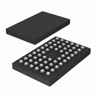
IC BUFF DVR TRI-ST 16BIT 56VFBGA
Manufacturer
NXP Semiconductors
Series
74LVTr
Datasheet
1.74LVT16244BDGG512.pdf
(18 pages)
Specifications of 74LVT16244BEV,118
Logic Type
Buffer/Line Driver, Non-Inverting
Number Of Elements
4
Number Of Bits Per Element
4
Current - Output High, Low
32mA, 64mA
Voltage - Supply
2.7 V ~ 3.6 V
Operating Temperature
-40°C ~ 85°C
Mounting Type
Surface Mount
Package / Case
56-VFBGA
Logic Family
LVT
Number Of Channels Per Chip
16
Polarity
Non-Inverting
Supply Voltage (max)
3.6 V
Supply Voltage (min)
2.7 V
Maximum Operating Temperature
+ 85 C
Mounting Style
SMD/SMT
High Level Output Current
- 32 mA
Low Level Output Current
64 mA
Minimum Operating Temperature
- 40 C
Number Of Lines (input / Output)
16 / 16
Output Type
3-State
Propagation Delay Time
1.8 ns at 3.3 V
Lead Free Status / RoHS Status
Lead free / RoHS Compliant
Other names
74LVT16244BEV-T
74LVT16244BEV-T
935270794118
74LVT16244BEV-T
935270794118
Available stocks
Company
Part Number
Manufacturer
Quantity
Price
Company:

Part Number:
74LVT16244BEV,118
Manufacturer:
NXP Semiconductors
Quantity:
10 000


NXP Semiconductors
Table 6.
At recommended operating conditions; voltages are referenced to GND (ground = 0 V).
[1]
[2]
[3]
[4]
[5]
[6]
10. Dynamic characteristics
Table 7.
Voltages are referenced to GND (ground = 0 V); for test circuit see
[1]
74LVT_LVTH16244B_8
Product data sheet
Symbol Parameter
I
ΔI
C
C
Symbol
T
t
t
t
t
t
t
CC
PLH
PHL
PZH
PZL
PHZ
PLZ
amb
I
O
CC
Typical values are measured at V
Unused pins at V
This is the bus hold overdrive current required to force the input to the opposite logic state.
This parameter is valid for any V
a transition time of 100 μs is permitted. This parameter is valid for T
I
This is the increase in supply current for each input at the specified voltage level other than V
Typical values are measured at V
CC
= −40 °C to +85 °C
is measured with outputs pulled to V
supply current
additional supply current
input capacitance
output capacitance
Static characteristics
Dynamic characteristics
Parameter
LOW to HIGH
propagation delay
HIGH to LOW
propagation delay
OFF-state to HIGH
propagation delay
OFF-state to LOW
propagation delay
HIGH to OFF-state
propagation delay
LOW to OFF-state
propagation delay
CC
or GND.
[1]
CC
CC
CC
…continued
between 0 V and 1.2 V with a transition time of up to 10 ms. From V
= 3.3 V and at T
= 3.3 V and T
Conditions
V
per input pin; V
at V
V
outputs disabled; V
Conditions
nAn to nYn; see
nAn to nYn; see
nOE to nYn; see
nOE to nYn; see
nOE to nYn; see
nOE to nYn; see
CC
I
CC
output HIGH
output LOW
outputs disabled
V
V
V
V
V
V
V
V
V
V
V
V
= 0 V or 3.0 V
CC
CC
CC
CC
CC
CC
CC
CC
CC
CC
CC
CC
CC
All information provided in this document is subject to legal disclaimers.
= 3.6 V; V
or GND.
= 2.7 V
= 3.0 V to 3.6 V
= 2.7 V
= 3.0 V to 3.6 V
= 2.7 V
= 3.0 V to 3.6 V
= 2.7 V
= 3.0 V to 3.6 V
= 2.7 V
= 3.0 V to 3.6 V
= 2.7 V
= 3.0 V to 3.6 V
− 0.6 V other inputs at V
amb
Rev. 08 — 22 March 2010
amb
I
= 25 °C.
CC
74LVT16244B; 74LVTH16244B
= GND or V
= 25 °C.
Figure 6
Figure 6
Figure 7
Figure 7
Figure 7
Figure 7
= 3.0 V to 3.6 V; one input
O
= 0 V or 3.0 V
amb
CC
Figure
; I
= 25 °C only.
CC
O
= 0 A
or GND
8.
Min
-
0.5
-
0.5
-
1.0
-
1.0
-
1.0
-
1.0
[5]
[6]
3.3 V 16-bit buffer/driver; 3-state
CC
Min
-
-
-
-
-
-
or GND.
Typ
-
-
-
-
-
-
1.8
1.7
2.3
2.1
3.2
2.9
CC
= 1.2 V to V
Typ
0.07
4.0
0.07
0.1
3
9
Max
4.0
3.2
4.0
3.2
5.0
4.0
5.3
4.0
5.0
4.5
4.4
4.0
© NXP B.V. 2010. All rights reserved.
CC
Max
0.12
6.0
0.12
0.2
-
-
= 3.3 V ± 0.3 V
Unit
ns
ns
ns
ns
ns
ns
ns
ns
ns
ns
ns
ns
Unit
mA
mA
mA
mA
pF
pF
8 of 18
Related parts for 74LVT16244BEV,118
Image
Part Number
Description
Manufacturer
Datasheet
Request
R

Part Number:
Description:
3.3V LVT 16-bit buffer/driver 3-State
Manufacturer:
PHILIPS [NXP Semiconductors]
Datasheet:

Part Number:
Description:
NXP Semiconductors designed the LPC2420/2460 microcontroller around a 16-bit/32-bitARM7TDMI-S CPU core with real-time debug interfaces that include both JTAG andembedded trace
Manufacturer:
NXP Semiconductors
Datasheet:

Part Number:
Description:
NXP Semiconductors designed the LPC2458 microcontroller around a 16-bit/32-bitARM7TDMI-S CPU core with real-time debug interfaces that include both JTAG andembedded trace
Manufacturer:
NXP Semiconductors
Datasheet:
Part Number:
Description:
NXP Semiconductors designed the LPC2468 microcontroller around a 16-bit/32-bitARM7TDMI-S CPU core with real-time debug interfaces that include both JTAG andembedded trace
Manufacturer:
NXP Semiconductors
Datasheet:
Part Number:
Description:
NXP Semiconductors designed the LPC2470 microcontroller, powered by theARM7TDMI-S core, to be a highly integrated microcontroller for a wide range ofapplications that require advanced communications and high quality graphic displays
Manufacturer:
NXP Semiconductors
Datasheet:
Part Number:
Description:
NXP Semiconductors designed the LPC2478 microcontroller, powered by theARM7TDMI-S core, to be a highly integrated microcontroller for a wide range ofapplications that require advanced communications and high quality graphic displays
Manufacturer:
NXP Semiconductors
Datasheet:
Part Number:
Description:
The Philips Semiconductors XA (eXtended Architecture) family of 16-bit single-chip microcontrollers is powerful enough to easily handle the requirements of high performance embedded applications, yet inexpensive enough to compete in the market for hi
Manufacturer:
NXP Semiconductors
Datasheet:
Part Number:
Description:
The XA-S3 device is a member of Philips Semiconductors? XA(eXtended Architecture) family of high performance 16-bitsingle-chip microcontrollers
Manufacturer:
NXP Semiconductors
Datasheet:

Part Number:
Description:
The NXP BlueStreak LH75401/LH75411 family consists of two low-cost 16/32-bit System-on-Chip (SoC) devices
Manufacturer:
NXP Semiconductors
Datasheet:
Part Number:
Description:
The NXP LPC3130/3131 combine an 180 MHz ARM926EJ-S CPU core, high-speed USB2
Manufacturer:
NXP Semiconductors
Datasheet:
Part Number:
Description:
The NXP LPC3141 combine a 270 MHz ARM926EJ-S CPU core, High-speed USB 2
Manufacturer:
NXP Semiconductors
Part Number:
Description:
The NXP LPC3143 combine a 270 MHz ARM926EJ-S CPU core, High-speed USB 2
Manufacturer:
NXP Semiconductors

Part Number:
Description:
The NXP LPC3152 combines an 180 MHz ARM926EJ-S CPU core, High-speed USB 2
Manufacturer:
NXP Semiconductors
Part Number:
Description:
The NXP LPC3154 combines an 180 MHz ARM926EJ-S CPU core, High-speed USB 2
Manufacturer:
NXP Semiconductors