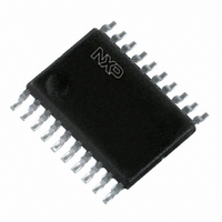
74HCT273PW,112 NXP Semiconductors, 74HCT273PW,112 Datasheet - Page 14

74HCT273PW,112
Manufacturer Part Number
74HCT273PW,112
Description
IC D-TYPE FF POS-EDG-TRG 20TSSOP
Manufacturer
NXP Semiconductors
Series
74HCTr
Type
D-Type Busr
Datasheet
1.74HC273PW118.pdf
(26 pages)
Specifications of 74HCT273PW,112
Function
Master Reset
Output Type
Non-Inverted
Number Of Elements
1
Number Of Bits Per Element
8
Frequency - Clock
36MHz
Delay Time - Propagation
15ns
Trigger Type
Positive Edge
Current - Output High, Low
4mA, 4mA
Voltage - Supply
4.5 V ~ 5.5 V
Operating Temperature
-40°C ~ 125°C
Mounting Type
Surface Mount
Package / Case
20-TSSOP
Logic Family
HCT
Technology
CMOS
Number Of Bits
8
Number Of Elements
1
Clock-edge Trigger Type
Positive-Edge
Polarity
Non-Inverting
Operating Supply Voltage (typ)
5V
Package Type
TSSOP
Propagation Delay Time
51ns
Low Level Output Current
4mA
High Level Output Current
-4mA
Frequency (max)
20MHz
Operating Supply Voltage (min)
4.5V
Operating Supply Voltage (max)
5.5V
Operating Temp Range
-40C to 125C
Operating Temperature Classification
Automotive
Mounting
Surface Mount
Pin Count
20
Lead Free Status / RoHS Status
Lead free / RoHS Compliant
Other names
74HCT273PW
74HCT273PW
935185820112
74HCT273PW
935185820112
Philips Semiconductors
Table 9:
Voltages are referenced to GND (ground = 0 V); t
Figure
[1]
Table 10:
Voltages are referenced to GND (ground = 0 V); t
Figure
74HC_HCT273_3
Product data sheet
Symbol Parameter
t
t
t
f
Symbol Parameter
T
t
t
t
t
t
t
rec
su
h
max
PHL
PLH
PHL
THL
TLH
W
amb
,
,
C
P
f
f
C
V
N = number of inputs switching;
i
o
D
CC
PD
= input frequency in MHz;
L
(C
= 25 C
= output frequency in MHz;
10.
10.
= output load capacitance in pF;
= C
L
is used to determine the dynamic power dissipation (P
= supply voltage in V;
recovery time MR to CP
set-up time Dn to CP
hold time Dn to CP
maximum input clock frequency
propagation delay CP to Qn
HIGH-to-LOW propagation delay
MR to Qn
output transition time
pulse width
PD
V
Dynamic characteristics 74HC273
Dynamic characteristics 74HCT273
CC
clock HIGH or LOW
master reset LOW
2
V
CC
f
o
2
) = sum of outputs.
f
i
N + (C
L
V
CC
2
f
o
) where:
Conditions
see
see
see
see
Conditions
see
see
V
V
V
CC
CC
CC
V
V
V
V
V
V
V
V
V
V
V
V
V
V
V
V
…continued
r
r
CC
CC
CC
CC
CC
CC
CC
CC
CC
CC
CC
CC
CC
CC
CC
CC
Rev. 03 — 24 January 2006
Figure 8
Figure 9
Figure 9
Figure 7
Figure 7
Figure 8
= t
= t
= 4.5 V; see
= 4.5 V; see
= 4.5 V; see
= 2.0 V
= 4.5 V
= 6.0 V
= 2.0 V
= 4.5 V
= 6.0 V
= 2.0 V
= 4.5 V
= 6.0 V
= 2.0 V
= 4.5 V
= 6.0 V
= 4.5 V
= 5 V; C
= 4.5 V
= 5 V; C
f
f
= 6 ns; C
= 6 ns; C
D
in W).
L
L
Octal D-type flip-flop with reset; positive-edge trigger
= 15 pF
= 15 pF
Figure 7
Figure 7
Figure 8
L
L
= 50 pF unless otherwise specified; for test circuit see
= 50 pF unless otherwise specified; for test circuit see
74HC273; 74HCT273
Min
75
15
13
90
18
15
3
3
3
4.0
20
24
Min
-
-
-
-
-
16
16
© Koninklijke Philips Electronics N.V. 2006. All rights reserved.
Typ
-
-
-
-
-
-
-
-
-
-
-
-
Typ
16
15
23
20
7
9
8
Max
30
-
34
-
15
-
-
Max
-
-
-
-
-
-
-
-
-
-
-
-
Unit
ns
ns
ns
ns
ns
ns
ns
14 of 26
Unit
ns
ns
ns
ns
ns
ns
ns
ns
ns
MHz
MHz
MHz


