74HC175DB,118 NXP Semiconductors, 74HC175DB,118 Datasheet - Page 2
74HC175DB,118
Manufacturer Part Number
74HC175DB,118
Description
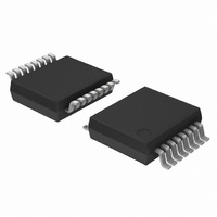
IC QUAD D F-F POS-EDGE 16SSOP
Manufacturer
NXP Semiconductors
Series
74HCr
Type
D-Type Busr
Datasheet
1.74HCT175D652.pdf
(13 pages)
Specifications of 74HC175DB,118
Function
Master Reset
Output Type
Differential
Number Of Elements
1
Number Of Bits Per Element
4
Frequency - Clock
89MHz
Delay Time - Propagation
16ns
Trigger Type
Positive Edge
Voltage - Supply
2 V ~ 6 V
Operating Temperature
-40°C ~ 125°C
Mounting Type
Surface Mount
Package / Case
16-SSOP
Lead Free Status / RoHS Status
Lead free / RoHS Compliant
Current - Output High, Low
-
Other names
74HC175DB-T
74HC175DB-T
935187390118
74HC175DB-T
935187390118


Philips Semiconductors
FEATURES
GENERAL DESCRIPTION
The 74HC/HCT175 are high-speed Si-gate CMOS devices
and are pin compatible with low power Schottky TTL
(LSTTL). They are specified in compliance with JEDEC
standard no. 7A.
QUICK REFERENCE DATA
GND = 0 V; T
Notes
1. C
2. For HC the condition is V
1998 Jul 08
SYMBOL
t
t
f
C
C
PHL
PLH
max
Four edge-triggered D flip-flops
Output capability: standard
I
I
PD
Quad D-type flip-flop with reset; positive-edge trigger
CC
f
f
C
V
For HCT the condition is V
i
o
CC
PD
= input frequency in MHz
L
category: MSI
= output frequency in MHz
(C
= output load capacitance in pF
P
= supply voltage in V
is used to determine the dynamic power dissipation (P
L
D
= C
V
amb
CC
PD
PARAMETER
propagation delay
propagation delay
maximum clock frequency
input capacitance
power dissipation capacitance per flip-flop notes 1 and 2
2
CP to Q
MR to Q
CP to Q
MR to Q
= 25 C; t
V
f
o
CC
) = sum of outputs
2
n
n
n
n
, Q
, Q
f
r
i
= t
n
n
I
I
f
= GND to V
= GND to V
= 6 ns
(C
L
V
CC
2
CC
CC
f
o
) where:
1.5 V
CONDITIONS
C
2
L
The 74HC/HCT175 have four edge-triggered, D-type
flip-flops with individual D inputs and both Q and Q
outputs.
The common clock (CP) and master reset (MR) inputs load
and reset (clear) all flip-flops simultaneously.
The state of each D input, one set-up time before the
LOW-to-HIGH clock transition, is transferred to the
corresponding output (Q
All Q
or data inputs by a LOW voltage level on the MR input.
The device is useful for applications where both the true
and complement outputs are required and the clock and
master reset are common to all storage elements.
= 15 pF; V
D
in W):
n
outputs will be forced LOW independently of clock
CC
= 5 V
n
HC
17
15
17
15
83
3.5
32
) of the flip-flop.
TYPICAL
74HC/HCT175
Product specification
HCT
16
19
16
16
54
3.5
34
UNIT
ns
ns
ns
ns
MHz
pF
pF
Related parts for 74HC175DB,118
Image
Part Number
Description
Manufacturer
Datasheet
Request
R

Part Number:
Description:
IC QUAD D F-F POS-EDGE 16SOIC
Manufacturer:
NXP Semiconductors
Datasheet:
Part Number:
Description:
IC QUAD D F-F POS-EDGE 16-SOIC
Manufacturer:
NXP Semiconductors
Datasheet:

Part Number:
Description:
NXP Semiconductors designed the LPC2420/2460 microcontroller around a 16-bit/32-bitARM7TDMI-S CPU core with real-time debug interfaces that include both JTAG andembedded trace
Manufacturer:
NXP Semiconductors
Datasheet:

Part Number:
Description:
NXP Semiconductors designed the LPC2458 microcontroller around a 16-bit/32-bitARM7TDMI-S CPU core with real-time debug interfaces that include both JTAG andembedded trace
Manufacturer:
NXP Semiconductors
Datasheet:
Part Number:
Description:
NXP Semiconductors designed the LPC2468 microcontroller around a 16-bit/32-bitARM7TDMI-S CPU core with real-time debug interfaces that include both JTAG andembedded trace
Manufacturer:
NXP Semiconductors
Datasheet:
Part Number:
Description:
NXP Semiconductors designed the LPC2470 microcontroller, powered by theARM7TDMI-S core, to be a highly integrated microcontroller for a wide range ofapplications that require advanced communications and high quality graphic displays
Manufacturer:
NXP Semiconductors
Datasheet:
Part Number:
Description:
NXP Semiconductors designed the LPC2478 microcontroller, powered by theARM7TDMI-S core, to be a highly integrated microcontroller for a wide range ofapplications that require advanced communications and high quality graphic displays
Manufacturer:
NXP Semiconductors
Datasheet:
Part Number:
Description:
The Philips Semiconductors XA (eXtended Architecture) family of 16-bit single-chip microcontrollers is powerful enough to easily handle the requirements of high performance embedded applications, yet inexpensive enough to compete in the market for hi
Manufacturer:
NXP Semiconductors
Datasheet:
Part Number:
Description:
The XA-S3 device is a member of Philips Semiconductors? XA(eXtended Architecture) family of high performance 16-bitsingle-chip microcontrollers
Manufacturer:
NXP Semiconductors
Datasheet:

Part Number:
Description:
The NXP BlueStreak LH75401/LH75411 family consists of two low-cost 16/32-bit System-on-Chip (SoC) devices
Manufacturer:
NXP Semiconductors
Datasheet:
Part Number:
Description:
The NXP LPC3130/3131 combine an 180 MHz ARM926EJ-S CPU core, high-speed USB2
Manufacturer:
NXP Semiconductors
Datasheet:
Part Number:
Description:
The NXP LPC3141 combine a 270 MHz ARM926EJ-S CPU core, High-speed USB 2
Manufacturer:
NXP Semiconductors
Part Number:
Description:
The NXP LPC3143 combine a 270 MHz ARM926EJ-S CPU core, High-speed USB 2
Manufacturer:
NXP Semiconductors

Part Number:
Description:
The NXP LPC3152 combines an 180 MHz ARM926EJ-S CPU core, High-speed USB 2
Manufacturer:
NXP Semiconductors