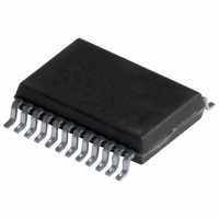
74ABT821DB,112 NXP Semiconductors, 74ABT821DB,112 Datasheet - Page 6

74ABT821DB,112
Manufacturer Part Number
74ABT821DB,112
Description
IC 10BIT D F-F POS-EDGE 24SSOP
Manufacturer
NXP Semiconductors
Series
74ABTr
Type
D-Type Busr
Datasheet
1.74ABT821PW112.pdf
(16 pages)
Specifications of 74ABT821DB,112
Function
Standard
Output Type
Tri-State Non Inverted
Number Of Elements
1
Number Of Bits Per Element
10
Frequency - Clock
125MHz
Delay Time - Propagation
4.1ns
Trigger Type
Negative Edge
Current - Output High, Low
32mA, 64mA
Voltage - Supply
4.5 V ~ 5.5 V
Operating Temperature
-40°C ~ 85°C
Mounting Type
Surface Mount
Package / Case
24-SSOP
Lead Free Status / RoHS Status
Lead free / RoHS Compliant
Other names
74ABT821DB
74ABT821DB
935069190112
74ABT821DB
935069190112
NXP Semiconductors
9. Static characteristics
Table 6.
[1]
[2]
[3]
[4]
74ABT821_4
Product data sheet
Symbol Parameter
V
V
V
V
I
I
I
I
I
I
I
ΔI
C
C
I
OFF
O(pu/pd)
OZ
LO
O
CC
IK
OH
OL
OL(pu)
I
O
CC
For valid test results, data must not be loaded into the flip-flops (or latches) after applying the power.
This parameter is valid for any V
transition time of up to 100 μs is permitted.
Not more than one output should be tested at a time, and the duration of the test should not exceed one second.
This is the increase in supply current for each input at 3.4 V.
input clamping voltage
HIGH-level output
voltage
LOW-level output
voltage
power-up LOW-level
output voltage
input leakage current
power-off leakage
current
power-up/power-down
output current
OFF-state output current V
output leakage current
output current
supply current
additional supply current per input pin; V
input capacitance
output capacitance
Static characteristics
CC
between 0 V and 2.1 V with a transition time of up to 10 ms. For V
Conditions
V
V
V
V
V
V
V
V
V
V
HIGH-state; V
V
V
V
input at 3.4 V; other inputs at V
or GND
V
outputs disabled; V
CC
I
CC
I
CC
I
CC
CC
CC
I
CC
CC
CC
CC
I
V
V
V
V
V
outputs HIGH-state
outputs LOW-state
outputs disabled
= V
= V
= GND or V
= GND or V
= 0 V or V
CC
CC
CC
O
O
= 4.5 V; I
= 4.5 V; I
= 5.5 V; I
= 5.5 V; V
= 0 V; V
= 2.0 V; V
= 5.5 V; V
= 5.5 V; V
= 5.5 V; V
= 5.5 V; V
All information provided in this document is subject to legal disclaimers.
= 2.7 V
= 0.5 V
IL
IL
= 4.5 V; I
= 5.0 V; I
= 4.5 V; I
or V
or V
IH
IH
I
CC
Rev. 04 — 26 March 2010
IK
OL
O
or V
O
CC
CC
I
O
I
I
O
I
CC
= 1 mA;
= GND or 5.5 V
= V
= GND or V
= GND or V
= −18 mA
OH
OH
OH
= 5.5 V;
= 0.5 V;
= 2.5 V
= 64 mA;
; OEn HIGH
O
= 5.5 V; one
= −3 mA
= −3 mA
= −32 mA
IL
O
≤ 4.5 V
or V
= 0 V or V
IH
10-bit D-type flip-flop; positive-edge trigger; 3-state
CC
CC
CC
CC
[1]
[2]
[3]
[4]
−180
−1.2
Min
2.5
3.0
2.0
-
-
-
-
-
-
-
-
-
-
-
-
-
-
25 °C
±0.01
−0.9
0.42
0.13
±5.0
±5.0
−5.0
Typ
−80
2.9
3.4
2.4
5.0
5.0
0.5
0.5
0.5
25
4
7
±100
Max
0.55
0.55
±1.0
±50
−50
−50
250
250
1.5
50
50
38
-
-
-
-
-
-
CC
= 2.1 V to V
−40 °C to +85 °C Unit
74ABT821
−180
−1.2
Min
2.5
3.0
2.0
-
-
-
-
-
-
-
-
-
-
-
-
-
-
© NXP B.V. 2010. All rights reserved.
CC
= 5 V ± 10 %, a
±100
Max
0.55
0.55
±1.0
±50
−50
−50
250
250
1.5
50
50
38
-
-
-
-
-
-
6 of 16
V
V
V
V
V
V
μA
μA
μA
μA
μA
μA
mA
μA
mA
μA
mA
pF
pF


