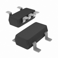
74AHC1G02GV,125 NXP Semiconductors, 74AHC1G02GV,125 Datasheet - Page 5

74AHC1G02GV,125
Manufacturer Part Number
74AHC1G02GV,125
Description
IC 2-IN NOR GATE SC74A-5
Manufacturer
NXP Semiconductors
Series
74AHCr
Datasheet
1.74AHC1G02GV125.pdf
(11 pages)
Specifications of 74AHC1G02GV,125
Number Of Circuits
1
Package / Case
SC-74-5, SOT-753
Logic Type
NOR Gate
Number Of Inputs
2
Current - Output High, Low
8mA, 8mA
Voltage - Supply
2 V ~ 5.5 V
Operating Temperature
-40°C ~ 125°C
Mounting Type
Surface Mount
Product
NOR
Logic Family
AHC
High Level Output Current
- 8 mA
Low Level Output Current
8 mA
Propagation Delay Time
3.2 ns
Supply Voltage (max)
5.5 V
Supply Voltage (min)
2 V
Maximum Operating Temperature
+ 125 C
Mounting Style
SMD/SMT
Minimum Operating Temperature
- 40 C
Lead Free Status / RoHS Status
Lead free / RoHS Compliant
Lead Free Status / RoHS Status
Lead free / RoHS Compliant, Lead free / RoHS Compliant
Other names
568-4541-2
74AHC1G02GV
74AHC1G02GV
935271650125
74AHC1G02GV
74AHC1G02GV
935271650125
NXP Semiconductors
Table 7.
Voltages are referenced to GND (ground = 0 V).
11. Dynamic characteristics
Table 8.
GND = 0 V; t
[1]
[2]
[3]
[4]
74AHC_AHCT1G02_6
Product data sheet
Symbol Parameter
I
C
Symbol Parameter
For type 74AHC1G02
t
C
For type 74AHCT1G02
t
C
CC
pd
pd
I
I
PD
PD
CC
t
Typical values are measured at V
Typical values are measured at V
C
P
f
C
V
pd
i
D
CC
PD
= input frequency in MHz; f
L
is the same as t
= output load capacitance in pF;
= C
is used to determine the dynamic power dissipation P
= supply voltage in Volts.
supply current V
additional
supply current
input
capacitance
PD
propagation
delay
power
dissipation
capacitance
propagation
delay
power
dissipation
capacitance
Static characteristics
Dynamic characteristics
r
= t
V
CC
f
=
2
3.0 ns. For test circuit see
PLH
f
i
+
and t
Conditions
V
per input pin; V
other inputs at V
I
O
(C
Conditions
A and B to Y;
see
per buffer;
C
V
A and B to Y;
see
per buffer;
C
V
I
CC
I
I
= 0 A; V
L
L
= V
L
V
V
V
PHL
= GND to V
= GND to V
o
= 50 pF; f = 1 MHz;
= 50 pF; f = 1 MHz;
= 5.5 V
CC
CC
CC
Figure 5
Figure 5
C
C
C
C
C
C
= output frequency in MHz;
V
CC
.
L
L
L
L
L
L
CC
= 3.0 V to 3.6 V
= 4.5 V to 5.5 V
= 4.5 V to 5.5 V
CC
CC
= 15 pF
= 50 pF
= 15 pF
= 50 pF
= 15 pF
= 50 pF
or GND; I
…continued
2
CC
= 3.3 V.
= 5.0 V.
f
o
= 5.5 V
) where:
CC
CC
I
= 3.4 V;
CC
O
or GND;
= 0 A;
Figure
Rev. 06 — 30 May 2007
[1]
[2]
[3]
[4]
[1]
[3]
[4]
6.
D
( W).
Min
Min
-
-
-
-
-
-
-
-
-
-
-
74AHC1G02; 74AHCT1G02
25 C
25 C
Typ
Typ
4.4
6.3
3.2
4.6
3.5
4.9
1.5
18
19
-
-
Max
11.4
Max
1.35
7.9
5.5
7.5
5.5
7.5
1.0
10
-
-
40 C to +85 C
40 C to +85 C
Min
Min
1.0
1.0
1.0
1.0
1.0
1.0
-
-
-
-
-
Max
Max
9.5
6.5
8.5
6.5
8.5
1.5
10
10
13
-
-
40 C to +125 C Unit
40 C to +125 C Unit
Min
Min
1.0
1.0
1.0
1.0
1.0
1.0
-
-
-
-
-
© NXP B.V. 2007. All rights reserved.
2-input NOR gate
Max
Max
10.5
14.5
1.5
7.0
9.5
7.0
9.5
40
10
-
-
5 of 11
mA
pF
ns
ns
ns
ns
pF
ns
ns
pF
A


