HCF4001BEY STMicroelectronics, HCF4001BEY Datasheet - Page 3
HCF4001BEY
Manufacturer Part Number
HCF4001BEY
Description
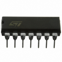
IC GATE NOR QUAD 2INP 14-DIP
Manufacturer
STMicroelectronics
Series
4000Br
Specifications of HCF4001BEY
Logic Type
NOR Gate
Number Of Inputs
2
Number Of Circuits
4
Current - Output High, Low
6.8mA, 6.8mA
Voltage - Supply
3 V ~ 20 V
Operating Temperature
-55°C ~ 125°C
Mounting Type
Through Hole
Package / Case
14-DIP (0.300", 7.62mm)
Logic Family
4000B
Logical Function
NOR
Number Of Elements
4
High Level Output Current
-2.4mA
Low Level Output Current
2.4mA
Propagation Delay Time
80ns
Operating Supply Voltage (typ)
3.3/5/9/12/15/18V
Operating Temp Range
-55C to 125C
Package Type
PDIP
Number Of Outputs
1
Technology
CMOS
Mounting
Through Hole
Pin Count
14
Operating Temperature Classification
Military
Quiescent Current
5uA
Operating Supply Voltage (max)
20V
Operating Supply Voltage (min)
3V
Product
NOR
Supply Voltage (max)
20 V
Supply Voltage (min)
3 V
Maximum Operating Temperature
+ 125 C
Mounting Style
Through Hole
Minimum Operating Temperature
- 55 C
Circuit Type
Monolithic Integrated
Current, Supply
150 μA
Function Type
2-Inputs
Logic Function
NOR Gate
Temperature, Operating, Range
-55 to +125 °C
Voltage, Supply
3 to 20 V
Output Current
6.8mA
No. Of Inputs
2
Supply Voltage Range
3V To 20V
Logic Case Style
DIP
No. Of Pins
14
Operating Temperature Range
-55°C To +125°C
Ic Generic Number
4001
Rohs Compliant
Yes
Lead Free Status / RoHS Status
Lead free / RoHS Compliant
Other names
497-1340-5
Available stocks
Company
Part Number
Manufacturer
Quantity
Price
Company:

Part Number:
HCF4001BEY
Manufacturer:
ST
Quantity:
15 000


DC SPECIFICATIONS
The Noise Margin for both "1" and "0" level is: 1V min. with V
DYNAMIC ELECTRICAL CHARACTERISTICS (T
(*) Typical temperature coefficient for all V
Symbol
t
t
Symbol
PLH
TLH
V
V
V
I
V
I
OH
C
OL
I
OH
I
OL
L
IH
IL
I
I
t
t
THL
PHL
Quiescent Current
High Level Output
Voltage
Low Level Output
Voltage
High Level Input
Voltage
Low Level Input
Voltage
Output Drive
Current
Output Sink
Current
Input Leakage
Current
Input Capacitance
Output Transition Time
Propagation Delay Time
Parameter
Parameter
0/10
0/15
0/20
0/10
0/15
10/0
15/0
0/10
0/15
0/10
0/15
0/18
(V)
0/5
0/5
5/0
0/5
0/5
0/5
V
I
DD
Test Condition
1.5/13.5
13.5/1.5
value is 0.3%/°C.
0.5/4.5
4.5/0.5
13.5
(V)
1/9
9/1
2.5
4.6
9.5
0.4
0.5
1.5
Any Input
Any Input
V
V
O
DD
10
15
10
15
5
5
(V)
( A)
|I
<1
<1
<1
<1
<1
<1
<1
<1
<1
<1
<1
<1
<1
<1
<1
<1
<1
<1
<1
O
|
DD
=5V, 2V min. with V
V
(V)
10
15
20
10
15
10
15
10
15
10
15
10
15
10
15
18
5
5
5
5
5
5
5
5
DD
Test Condition
amb
14.95
-1.36
-0.44
Min.
4.95
9.95
0.44
-1.1
-3.0
= 25°C, C
3.5
1.1
3.0
11
7
T
A
Typ.
0.01
0.01
0.01
0.02
0.05
0.05
0.05
= 25°C
-3.2
-2.6
-6.8
2.6
6.8
10
-1
1
5
DD
-5
=10V, 2.5V min. with V
L
= 50pF, R
Max.
0.25
0.5
1.5
7.5
0.1
1
5
3
4
Value
14.95
-1.15
-0.36
Min.
-40 to 85°C
4.95
9.95
0.36
-0.9
-2.4
3.5
0.9
2.4
11
7
L
= 200K , t
Max.
Min.
0.05
0.05
0.05
150
7.5
1.5
15
30
3
4
DD
1
=15V
Value (*)
-55 to 125°C
14.95
-0.36
Min.
4.95
9.95
0.36
Typ.
-1.1
-0.9
-2.4
125
100
3.5
0.9
2.4
60
45
50
40
11
7
r
= t
HCF4001B
Max.
f
Max.
0.05
0.05
0.05
150
250
120
200
100
7.5
1.5
15
30
= 20 ns)
90
80
3
4
1
Unit
Unit
mA
mA
pF
ns
ns
V
V
V
V
A
A
3/8
Related parts for HCF4001BEY
Image
Part Number
Description
Manufacturer
Datasheet
Request
R

Part Number:
Description:
NOR GATE
Manufacturer:
STMICROELECTRONICS [STMicroelectronics]
Datasheet:

Part Number:
Description:
STMicroelectronics [RIPPLE-CARRY BINARY COUNTER/DIVIDERS]
Manufacturer:
STMicroelectronics
Datasheet:
Part Number:
Description:
STMicroelectronics [LIQUID-CRYSTAL DISPLAY DRIVERS]
Manufacturer:
STMicroelectronics
Datasheet:

Part Number:
Description:
BOARD EVAL FOR MEMS SENSORS
Manufacturer:
STMicroelectronics
Datasheet:
Part Number:
Description:
NPN TRANSISTOR POWER MODULE
Manufacturer:
STMicroelectronics
Datasheet:
Part Number:
Description:
TURBOSWITCH ULTRA-FAST HIGH VOLTAGE DIODE
Manufacturer:
STMicroelectronics
Datasheet:
Part Number:
Description:
Manufacturer:
STMicroelectronics
Datasheet:
Part Number:
Description:
DIODE / SCR MODULE
Manufacturer:
STMicroelectronics
Datasheet:
Part Number:
Description:
DIODE / SCR MODULE
Manufacturer:
STMicroelectronics
Datasheet:
Part Number:
Description:
Search -----> STE16N100
Manufacturer:
STMicroelectronics
Datasheet:
Part Number:
Description:
Search ---> STE53NA50
Manufacturer:
STMicroelectronics
Datasheet:
Part Number:
Description:
NPN Transistor Power Module
Manufacturer:
STMicroelectronics
Datasheet: