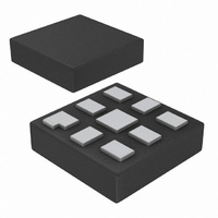
74LVC2G00GM,125 NXP Semiconductors, 74LVC2G00GM,125 Datasheet - Page 9

74LVC2G00GM,125
Manufacturer Part Number
74LVC2G00GM,125
Description
IC DUAL 2-IN NAND GATE 8-XQFN
Manufacturer
NXP Semiconductors
Series
74LVCr
Datasheet
1.74LVC2G00GT115.pdf
(20 pages)
Specifications of 74LVC2G00GM,125
Number Of Circuits
2
Package / Case
8-XQFN
Logic Type
NAND Gate
Number Of Inputs
2
Current - Output High, Low
32mA, 32mA
Voltage - Supply
1.65 V ~ 5.5 V
Operating Temperature
-40°C ~ 125°C
Mounting Type
Surface Mount
Logic Family
74LVC
High Level Output Current
- 32 mA
Low Level Output Current
32 mA
Propagation Delay Time
3 ns
Supply Voltage (max)
5.5 V
Supply Voltage (min)
1.65 V
Maximum Operating Temperature
+ 125 C
Mounting Style
SMD/SMT
Minimum Operating Temperature
- 40 C
Operating Temperature Range
- 40 C to + 125 C
Output Current
50 mA
Output Voltage
0 V to 5.5 V
Power Dissipation
300 mW
Lead Free Status / RoHS Status
Lead free / RoHS Compliant
Lead Free Status / RoHS Status
Lead free / RoHS Compliant, Lead free / RoHS Compliant
Other names
74LVC2G00GM-G
74LVC2G00GM-G
935277235125
74LVC2G00GM-G
935277235125
NXP Semiconductors
13. Package outline
Fig 10. Package outline SOT505-2 (TSSOP8)
74LVC2G00_9
Product data sheet
TSSOP8: plastic thin shrink small outline package; 8 leads; body width 3 mm; lead length 0.5 mm
DIMENSIONS (mm are the original dimensions)
Note
1. Plastic or metal protrusions of 0.15 mm maximum per side are not included.
UNIT
mm
VERSION
OUTLINE
SOT505-2
max.
1.1
A
0.15
0.00
A 1
8
1
0.95
0.75
A 2
y
pin 1 index
IEC
e
Z
0.25
A 3
D
0.38
0.22
b p
b p
All information provided in this document is subject to legal disclaimers.
0
5
0.18
0.08
4
JEDEC
c
- - -
w
REFERENCES
D
3.1
2.9
M
(1)
Rev. 09 — 8 June 2010
E
3.1
2.9
(1)
c
JEITA
scale
0.65
2.5
e
A
H E
4.1
3.9
A 2
A 1
0.5
L
H E
E
5 mm
0.47
0.33
detail X
L p
0.2
v
L
L p
PROJECTION
EUROPEAN
0.13
w
A
(A 3 )
Dual 2-input NAND gate
74LVC2G00
0.1
y
X
v
θ
M
0.70
0.35
Z
© NXP B.V. 2010. All rights reserved.
A
(1)
ISSUE DATE
02-01-16
8°
0°
θ
SOT505-2
9 of 20


