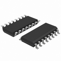
74LV259D,112 NXP Semiconductors, 74LV259D,112 Datasheet - Page 8

74LV259D,112
Manufacturer Part Number
74LV259D,112
Description
IC 8BIT ADDRESSABLE LATCH 16SOIC
Manufacturer
NXP Semiconductors
Series
74LVr
Datasheet
1.74LV259DB118.pdf
(19 pages)
Specifications of 74LV259D,112
Logic Type
D-Type, Addressable
Package / Case
16-SOIC (3.9mm Width)
Circuit
1:8
Output Type
Standard
Voltage - Supply
1 V ~ 3.6 V
Independent Circuits
1
Delay Time - Propagation
36ns
Current - Output High, Low
6mA, 6mA
Operating Temperature
-40°C ~ 125°C
Mounting Type
Surface Mount
Number Of Circuits
1
Logic Family
74LV
Polarity
Non-Inverting
High Level Output Current
- 6 mA
Low Level Output Current
6 mA
Propagation Delay Time
105 ns at 1.2 V, 36 ns at 2 V, 26 ns at 2.7 V
Supply Voltage (max)
3.6 V
Supply Voltage (min)
1 V
Maximum Operating Temperature
+ 125 C
Minimum Operating Temperature
- 40 C
Mounting Style
SMD/SMT
Lead Free Status / RoHS Status
Lead free / RoHS Compliant
Lead Free Status / RoHS Status
Lead free / RoHS Compliant, Lead free / RoHS Compliant
Other names
568-2947-5
935150550112
935150550112
NXP Semiconductors
Table 8.
GND = 0 V; For test circuit see
[1]
[2]
[3]
[4]
74LV259_3
Product data sheet
Symbol Parameter
t
t
t
C
su
h
h
PD
Typical values are measured at T
t
Typical value measured at V
C
P
f
f
C
V
N = number of inputs switching;
pd
i
o
D
CC
PD
= input frequency in MHz;
L
(C
= output frequency in MHz;
is the same as t
= output load capacitance in pF;
= C
L
is used to determine the dynamic power dissipation (P
= supply voltage in V;
set-up time
hold time
hold time
power dissipation
capacitance
PD
V
Dynamic characteristics
CC
2
V
CC
f
o
2
) = sum of outputs.
PLH
f
i
N + (C
and t
PHL
CC
Conditions
D, An to LE; see
Figure 11
V
V
V
V
D to LE; see
V
V
V
V
An to LE; see
V
V
V
V
C
V
Figure
CC
CC
CC
CC
CC
CC
CC
CC
CC
CC
CC
CC
I
L
L
.
= 3.3 V.
= GND to V
= 50 pF; f
amb
= 1.2 V
= 2.0 V
= 2.7 V
= 3.0 V to 3.6 V
= 1.2 V
= 2.0 V
= 2.7 V
= 3.0 V to 3.6 V
= 1.2 V
= 2.0 V
= 2.7 V
= 3.0 V to 3.6 V
V
CC
= 25 C.
12.
…continued
2
f
o
) where:
i
Figure 10
= 1 MHz;
Figure 11
CC
Figure 10
Rev. 03 — 2 January 2008
D
and
in W).
[3]
[3]
[3]
[4]
Min
24
18
14
5
5
5
5
5
5
-
-
-
40 C to +85 C
Typ
35
12
19
9
7
30
10
20
8
6
7
5
4
[1]
Max
-
-
-
-
-
-
-
-
-
-
-
-
8-bit addressable latch
40 C to +125 C
Min
29
21
17
5
5
5
5
5
5
-
-
-
© NXP B.V. 2008. All rights reserved.
74LV259
Max
-
-
-
-
-
-
-
-
-
-
-
-
8 of 19
Unit
ns
ns
ns
ns
ns
ns
ns
ns
ns
ns
ns
ns
pF


