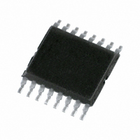
74LV259PW,118 NXP Semiconductors, 74LV259PW,118 Datasheet - Page 5

74LV259PW,118
Manufacturer Part Number
74LV259PW,118
Description
IC 8BIT ADDRESSABL LATCH 16TSSOP
Manufacturer
NXP Semiconductors
Series
74LVr
Datasheet
1.74LV259DB118.pdf
(19 pages)
Specifications of 74LV259PW,118
Logic Type
D-Type, Addressable
Package / Case
16-TSSOP
Circuit
1:8
Output Type
Standard
Voltage - Supply
1 V ~ 3.6 V
Independent Circuits
1
Delay Time - Propagation
36ns
Current - Output High, Low
6mA, 6mA
Operating Temperature
-40°C ~ 125°C
Mounting Type
Surface Mount
Number Of Circuits
1
Logic Family
LV
Polarity
Non-Inverting
High Level Output Current
- 6 mA
Low Level Output Current
6 mA
Propagation Delay Time
17 ns at 3.3 V
Supply Voltage (max)
3.6 V
Supply Voltage (min)
1 V
Maximum Operating Temperature
+ 125 C
Minimum Operating Temperature
- 40 C
Mounting Style
SMD/SMT
Lead Free Status / RoHS Status
Lead free / RoHS Compliant
Lead Free Status / RoHS Status
Lead free / RoHS Compliant, Lead free / RoHS Compliant
Other names
74LV259PW-T
74LV259PW-T
935174700118
74LV259PW-T
935174700118
NXP Semiconductors
7. Limiting values
Table 5.
In accordance with the Absolute Maximum Rating System (IEC 60134). Voltages are referenced to GND (ground = 0 V).
[1]
[2]
[3]
[4]
[5]
8. Recommended operating conditions
Table 6.
Voltages are referenced to GND (ground = 0 V).
[1]
74LV259_3
Product data sheet
Symbol
V
I
I
I
I
I
T
P
Symbol
V
V
V
T
IK
OK
O
CC
GND
stg
amb
t/ V
CC
tot
CC
I
O
The input and output voltage ratings may be exceeded if the input and output current ratings are observed.
P
P
P
P
The static characteristics are guaranteed from V
V
tot
tot
tot
tot
CC
derates linearly with 12 mW/K above 70 C.
derates linearly with 8 mW/K above 70 C.
derates linearly with 5.5 mW/K above 60 C.
derates linearly with 4.5 mW/K above 60 C.
= 1.0 V (with input levels GND or V
Limiting values
Recommended operating conditions
Parameter
supply voltage
input voltage
output voltage
ambient temperature
input transition rise and fall rate
Parameter
supply voltage
input clamping current
output clamping current
output current
supply current
ground current
storage temperature
total power dissipation
CC
).
CC
Conditions
V
V
V
Conditions
V
V
V
T
CC
CC
CC
= 1.2 V to V
Rev. 03 — 2 January 2008
amb
I
O
O
DIP16 package
SO16 package
(T)SSOP16 package
DHVQFN16 package
< 0.5 V or V
< 0.5 V or V
= 0.5 V to (V
= 1.0 V to 2.0 V
= 2.0 V to 2.7 V
= 2.7 V to 3.6 V
= 40 C to +125 C
CC
= 5.5 V, but LV devices are guaranteed to function down to
I
O
> V
CC
> V
CC
+ 0.5 V)
CC
+ 0.5 V
+ 0.5 V
[1]
Min
1.0
0
0
-
-
-
40
Typ
3.3
-
-
+25
-
-
-
[1]
[1]
[2]
[3]
[4]
[5]
Min
-
-
-
-
-
-
-
-
8-bit addressable latch
0.5
50
65
Max
3.6
V
V
+125
500
200
100
© NXP B.V. 2008. All rights reserved.
74LV259
CC
CC
Max
+4.6
50
-
+150
750
500
500
500
20
50
25
Unit
V
mA
mA
mA
mA
mA
mW
mW
mW
mW
Unit
V
V
V
ns/V
ns/V
ns/V
C
C
5 of 19


