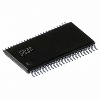
HSTL16918DGG,518 NXP Semiconductors, HSTL16918DGG,518 Datasheet - Page 4

HSTL16918DGG,518
Manufacturer Part Number
HSTL16918DGG,518
Description
IC MEMORY ADDRESS LATCH 48TSSOP
Manufacturer
NXP Semiconductors
Series
HSTLr
Datasheet
1.HSTL16918DGG518.pdf
(8 pages)
Specifications of HSTL16918DGG,518
Logic Type
D-Type Latch
Circuit
9:18
Output Type
Tri-State
Voltage - Supply
3.15 V ~ 3.45 V
Independent Circuits
1
Delay Time - Propagation
3.4ns
Current - Output High, Low
24mA, 24mA
Operating Temperature
0°C ~ 70°C
Mounting Type
Surface Mount
Package / Case
48-TSSOP
Lead Free Status / RoHS Status
Lead free / RoHS Compliant
Other names
935270253518
HSTL16918DGG-T
HSTL16918DGG-T
HSTL16918DGG-T
HSTL16918DGG-T
1. Stresses beyond those listed may cause permanent damage to the device. These are stress ratings only and functional operation of the
2. The input and output negative-voltage ratings may be exceeded if the input and output clamp-current ratings are observed.
3. This current flows only when the output is in the high state and V
4. The package thermal impedance is calculated in accordance with JESD 51.
1. All unused inputs of the device must be held at V
Philips Semiconductors
ABSOLUTE MAXIMUM RATINGS
Over operating free-air temperature range (unless otherwise noted).
NOTES:
RECOMMENDED OPERATING CONDITIONS
NOTE:
2001 Jun 16
SYMBOL
SYMBOL
SYMBOL
9-bit to 18-bit HSTL-to-LVTTL memory address latch
device at these or any other conditions beyond those indicated under “recommended operating conditions” is not implied. Exposure to
absolute-maximum-rated conditions for extended periods may affect device reliability.
V
T
V
V
T
I
V
V
I
V
V
V
I
I
REF
amb
V
OK
I
V
OH
OL
CC
IK
stg
CC
O
JA
IH
IH
IL
IL
O
I
I
Supply voltage range
Input voltage range
Output voltage range
Input clamp current
Output clamp current
Continuous output current
Continuous current through each V
Package thermal impedance
Storage temperature range
Supply voltage
Reference voltage
Input voltage
AC high-level input voltage
AC low-level input voltage
DC high-level input voltage
DC low-level input voltage
High-level output current
Low-level output current
Operating free-air temperature range
PARAMETER
2
2
3
PARAMETER
PARAMETER
1
4
CC
CC
or GND
or GND to ensure proper device operation.
1
All inputs
All inputs
All inputs
All inputs
O
> V
4
CC
V
.
O
CONDITIONS
V
< 0 or V
O
V
V
= 0 to V
REF
REF
V
I
< 0
3.15
0.68
Min
+ 200 mV
+ 100 mV
O
0
0
> V
CC
CC
LIMITS
Nom
0.75
–0.5 to V
–0.5 to V
–0.5 to +4.6
–65 to +150
RATING
V
V
REF
REF
–50
100
89
50
50
CC
CC
Max
3.45
– 200 mV
– 100 mV
–24
+70
0.9
1.5
24
HSTL16918
+0.5
+0.5
Product data
UNIT
UNIT
UNIT
mA
mA
mA
mA
C/W
mA
mA
V
V
V
V
V
V
V
V
V
V
C
C


