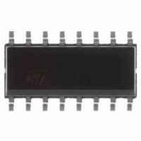
M74HC221RM13TR STMicroelectronics, M74HC221RM13TR Datasheet

M74HC221RM13TR
Specifications of M74HC221RM13TR
Related parts for M74HC221RM13TR
M74HC221RM13TR Summary of contents
Page 1
... MONOSTABLE period longer. Limit for values of Cx and LIMIT 0.7 All inputs are equipped with protection circuits against static discharge and transient excess voltage. M74HC221 DIP SOP TUBE M74HC221B1R M74HC221M1R M74HC221RM13TR M74HC221TTR the output maintains < 3. > 3. TSSOP T & R the ...
Page 2
M74HC221 INPUT AND OUTPUT EQUIVALENT CIRCUIT TRUTH TABLE INPUTS Don’t Care (*) : Except for monostable period 2/14 PIN DESCRIPTION PIN ...
Page 3
SYSTEM DIAGRAM This logic diagram has not be used to estimate propagation delays TIMING CHART M74HC221 3/14 ...
Page 4
M74HC221 BLOCK DIAGRAM (1) Cx, Rx, Dx are external components. ( clamping diode. The external capacitor is charged to Vcc in the stand-by-state, i.e. no trigger. When the supply voltage is turned off scharged ...
Page 5
ABSOLUTE MAXIMUM RATINGS Symbol V Supply Voltage Input Voltage Output Voltage Input Diode Current Output Diode Current Output Current ...
Page 6
M74HC221 DC SPECIFICATIONS Symbol Parameter V V High Level Input IH Voltage V Low Level Input IL Voltage V High Level Output OH Voltage (Q, Q Output) V Low Level Output OL Voltage (Q, Q Output) I Input Leakage I ...
Page 7
AC ELECTRICAL CHARACTERISTICS (C Symbol Parameter Output Transition TLH THL Time t t Propagation Delay PLH PHL Time ( Propagation Delay PLH PHL Time(CLR TRIGGER - Propagation ...
Page 8
M74HC221 TEST CIRCUIT C = 50pF or equivalent (includes jig and probe capacitance pulse generator (typically OUT WAVEFORM 1: MINIMUM PULSE WIDTH (A, B), OUTPUT PULSE WIDTH, PROPAGATION DELAY TIME (f=1MHz; 50% ...
Page 9
WAVEFORM 2 : MIIMUM PULSE WIDTH (CLR), PROPAGATION DELAY TIME(f=1MHz; 50% duty cycle) M74HC221 9/14 ...
Page 10
M74HC221 WAVEFORM 3 : REMOVAL TIME (CLR TO A-B) (f=1MHz; 50% duty cycle) WAVEFORM 4 : REMOVAL TIME (CLR TO A-B) (f=1MHz; 50% duty cycle) 10/14 ...
Page 11
Plastic DIP-16 (0.25) MECHANICAL DATA mm. DIM. MIN. a1 0. 17. TYP MAX. MIN. 0.020 1.65 0.030 0.5 0.25 20 8.5 2.54 7.1 5.1 3.3 1.27 M74HC221 inch ...
Page 12
M74HC221 DIM. MIN 0 0. 9 3.8 G 4 12/14 SO-16 MECHANICAL DATA mm. TYP MAX. 1.75 0.2 1.65 0.46 0.25 0.5 ...
Page 13
TSSOP16 MECHANICAL DATA DIM. MIN 0.05 A2 0.8 b 0.19 c 0.09 D 4.9 E 6 0° PIN 1 IDENTIFICATION 1 mm. TYP MAX. 1.2 0.15 1 1.05 ...
Page 14
... No license is granted by implication or otherwise under any patent or patent rights of STMicroelectronics. Specifications mentioned in this publication are subject to change without notice. This publication supersedes and replaces all information previously supplied ...


