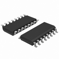
74HC221D,653 NXP Semiconductors, 74HC221D,653 Datasheet - Page 2

74HC221D,653
Manufacturer Part Number
74HC221D,653
Description
IC DUAL MULTI-VIBRATOR 16SOIC
Manufacturer
NXP Semiconductors
Series
74HCr
Datasheet
1.74HCT221D112.pdf
(15 pages)
Specifications of 74HC221D,653
Logic Type
Monostable
Package / Case
16-SOIC (3.9mm Width)
Independent Circuits
2
Schmitt Trigger Input
Yes
Propagation Delay
19ns
Voltage - Supply
2 V ~ 6 V
Operating Temperature
-40°C ~ 125°C
Mounting Type
Surface Mount
Elements Per Chip
2
Logic Family
HC
Input Bias Current (max)
0.008 mA
Propagation Delay Time
220 ns, 44 ns, 37 ns
High Level Output Current
- 5.2 mA
Low Level Output Current
5.2 mA
Supply Voltage (max)
6 V
Supply Voltage (min)
2 V
Maximum Operating Temperature
+ 125 C
Minimum Operating Temperature
- 40 C
Mounting Style
SMD/SMT
Operating Supply Voltage
5 V
Lead Free Status / RoHS Status
Lead free / RoHS Compliant
Current - Output High, Low
-
Lead Free Status / Rohs Status
Lead free / RoHS Compliant
Other names
74HC221D-T
74HC221D-T
933714630653
74HC221D-T
933714630653
Philips Semiconductors
FEATURES
GENERAL DESCRIPTION
The 74HC/HCT221 are high-speed Si-gate CMOS devices
and are pin compatible with low power Schottky TTL
(LSTTL). They are specified in compliance with JEDEC
standard no. 7A.
The 74HC/HCT221 are dual non-retriggerable monostable
multivibrators. Each multivibrator features an active
LOW-going edge input (nA) and an active HIGH-going
edge input (nB), either of which can be used as an enable
input.
Pulse triggering occurs at a particular voltage level and is
not directly related to the transition time of the input pulse.
Schmitt-trigger input circuitry for the nB inputs allow
QUICK REFERENCE DATA
GND = 0 V; T
Notes
1. C
2. For HC the condition is V
December 1990
SYMBOL PARAMETER
t
t
C
C
PHL
PLH
Pulse width variance is typically less than
Pin-out identical to “123”
Overriding reset terminates output pulse
nB inputs have hysteresis for improved noise immunity
Output capability: standard (except for nR
I
Dual non-retriggerable monostable
multivibrator with reset
I
PD
CC
f
C
V
For HCT the condition is V
i
CC
PD
= input frequency in MHz; f
EXT
category: MSI
(C
P
L
= supply voltage in V; D = duty factor in %
is used to determine the dynamic power dissipation (P
D
= timing capacitance in pF; C
= C
V
propagation delay
input capacitance
power dissipation capacitance per package notes 1 and 2
CC
amb
PD
nA, nB, nR
nA, nB, nR
2
= 25 C; t
V
f
o
CC
) = sum of outputs
2
D
D
f
r
i
to nQ, nQ
to nQ, nQ
= t
I
= GND to V
I
f
= GND to V
= 6 ns
(C
o
L
= output frequency in MHz
V
L
CC
= output load capacitance in pF
2
CC
CC
EXT
f
o
5%
) 0.33 C
/C
1.5 V
EXT
)
C
R
CONDITIONS
EXT
2
L
EXT
= 15 pF; V
jitter-free triggering from inputs with slow transition rates,
providing the circuit with excellent noise immunity.
Once triggered, the outputs (nQ, nQ) are independent of
further transitions of nA and nB inputs and are a function
of the timing components. The output pulses can be
terminated by the overriding active LOW reset inputs
(nR
output pulse.
Pulse width stability is achieved through internal
compensation and is virtually independent of V
temperature. In most applications pulse stability will only
be limited by the accuracy of the external timing
components.
The output pulse width is defined by the following
relationship:
t
t
Pin assignments for the “221” are identical to those of the
“123” so that the “221” can be substituted for those
products in systems not using the retrigger by merely
changing the value of R
W
W
D
= 5 k ; C
V
= C
= 0.7C
in W):
D
CC
). Input pulses may be of any duration relative to the
EXT
2
EXT
R
CC
f
o
EXT
EXT
R
= 5 V;
D 28 V
EXT
In
= 0 pF
2
EXT
CC
and/or C
where:
29
35
3.5
90
HC
74HC/HCT221
TYPICAL
Product specification
EXT
32
36
3.5
96
.
HCT
CC
ns
ns
pF
pF
and
UNIT


