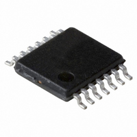
CBT3125PW,112 NXP Semiconductors, CBT3125PW,112 Datasheet - Page 5

CBT3125PW,112
Manufacturer Part Number
CBT3125PW,112
Description
IC FET BUS SWITCH QUAD 14TSSOP
Manufacturer
NXP Semiconductors
Series
74CBTr
Type
FET Bus Switchr
Datasheet
1.CBT3125DB118.pdf
(10 pages)
Specifications of CBT3125PW,112
Circuit
1 x 1:1
Independent Circuits
4
Current - Output High, Low
15mA, 64mA
Voltage Supply Source
Single Supply
Voltage - Supply
4.5 V ~ 5.5 V
Operating Temperature
-40°C ~ 85°C
Mounting Type
Surface Mount
Package / Case
14-TSSOP
Logic Family
CBT
Number Of Bits
4
Number Of Elements
4
Technology
CMOS
High Level Output Current
-128mA
Low Level Output Current
128mA
On Resistance
10Ohm
Propagation Delay Time
5.4ns
Package Type
TSSOP
Operating Temp Range
-40C to 85C
Operating Temperature Classification
Industrial
Operating Supply Voltage (min)
4.5V
Operating Supply Voltage (typ)
5V
Operating Supply Voltage (max)
5.5V
Quiescent Current
3uA
Pin Count
14
Mounting
Surface Mount
Lead Free Status / RoHS Status
Lead free / RoHS Compliant
Other names
935270670112
CBT3125PWDH
CBT3125PWDH
CBT3125PWDH
CBT3125PWDH
t
t
t
Philips Semiconductors
AC WAVEFORMS
V
2001 Dec 12
PLH
PLZ
PZL
M
Output Control
Quadruple FET bus switch
OUTPUT
Waveform 1
Waveform 2
= 1.5 V, V
INPUT
S1 at Open
(see Note)
(see Note)
and t
and t
and t
S1 at 7 V
Output
Output
Waveform 1. Input to Output Propagation Delays
Waveform 2. Output Enable and Disable Times
PHZ
PZH
PHL
Note:
Waveform 1 is for an output with internal conditions such that
the output is low except when disabled by the output control.
Waveform 2 is for an output with internal conditions such that
the output is high except when disabled by the output control.
t
PZH
IN
t
PZL
are the same as t
are the same as t
are the same as t
= GND to 3.0V
1.5 V
t
PLH
1.5 V
1.5 V
1.5 V
1.5 V
pd
dis
en
.
.
.
t
PHZ
t
PLZ
1.5 V
1.5 V
t
PHL
V
V
OL
OH
+ 0.3 V
– 0.3 V
1.5 V
SA00558
SA00028
3 V
0 V
3.5 V
V
V
0 V
OL
OH
3 V
0 V
V
V
OH
OL
5
t
t
1. All input pulses are supplied by generators having the following
2. The outputs are measured one at a time with one transition per
TEST CIRCUIT
NOTES:
PLZ
PZL
characteristics: PRR
t
measurement.
f
and t
and t
2.5 ns.
From Output
DEFINITIONS
C
Under Test
PHZ
PZH
L
=
are the same as t
are the same as t
C
Load capacitance includes jig and probe capacitance;
see AC CHARACTERISTICS for value.
L
= 50 pF
t
t
PHZ
10 MHz, Z
PLZ
TEST
t
pd
/t
/t
PZL
PZH
dis
en
500
Load Circuit
.
.
500
O
= 50 , t
open
open
7 V
S1
S1
r
CBT3125
7 V
GND
SA00012
2.5 ns,
Open
Product data


