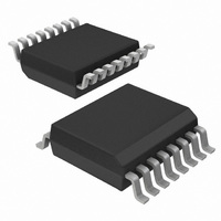
CBT3126DS,118 NXP Semiconductors, CBT3126DS,118 Datasheet - Page 4

CBT3126DS,118
Manufacturer Part Number
CBT3126DS,118
Description
IC FET BUS SWITCH QUAD 16QSOP
Manufacturer
NXP Semiconductors
Series
74CBTr
Type
FET Bus Switchr
Datasheet
1.CBT3126DB118.pdf
(13 pages)
Specifications of CBT3126DS,118
Circuit
1 x 1:1
Independent Circuits
4
Current - Output High, Low
15mA, 64mA
Voltage Supply Source
Single Supply
Voltage - Supply
4.5 V ~ 5.5 V
Operating Temperature
-40°C ~ 85°C
Mounting Type
Surface Mount
Package / Case
16-QSOP
Logic Family
CBT
Number Of Bits
4
Number Of Elements
4
Technology
CMOS
High Level Output Current
-128mA
Low Level Output Current
128mA
Package Type
SSOP
Operating Temp Range
-40C to 85C
Operating Temperature Classification
Industrial
Operating Supply Voltage (min)
4.5V
Operating Supply Voltage (typ)
5V
Operating Supply Voltage (max)
5.5V
Quiescent Current
3uA
Pin Count
16
Mounting
Surface Mount
Lead Free Status / RoHS Status
Lead free / RoHS Compliant
Other names
935270736118
CBT3126DS-T
CBT3126DS-T
CBT3126DS-T
CBT3126DS-T
NXP Semiconductors
9. Static characteristics
Table 6.
T
[1]
[2]
[3]
10. Dynamic characteristics
Table 7.
T
[1]
[2]
CBT3126_4
Product data sheet
Symbol
V
V
I
I
C
C
R
Symbol
t
t
t
I
CC
pd
en
dis
amb
amb
I
IK
pass
I
io(off)
ON
CC
All typical values are measured at V
This is the increase in supply current for each input that is at the specified TTL voltage level rather than V
Measured by the voltage drop between the A and the B terminals at the indicated current through the switch. ON resistance is
determined by the lowest voltage of the two (A or B) terminals.
This parameter is warranted but not production tested. The propagation delay is based on the RC time constant of the typical ON
resistance of the switch and a load capacitance, when driven by an ideal voltage source (zero output impedance).
t
t
t
PLH
PZL
PLZ
= 40 C to +85 C.
= 40 C to +85 C; V
and t
and t
and t
Static characteristics
Dynamic characteristics
Parameter
input clamping voltage
pass voltage
input leakage current
supply current
additional supply current
input capacitance
off-state input/output capacitance
ON resistance
PZH
PHZ
PHL
Parameter
propagation delay
enable time
disable time
are the same as t
are the same as t
are the same as t
CC
= 4.5 V to 5.5 V; for test circuit see
pd
en
dis
;
;
.
CC
Conditions
nA to nB or nB to nA; see
nOE to nA or nB; see
nOE to nA or nB; see
= 5 V; T
amb
Conditions
V
V
V
V
V
control pins; per input;
V
other inputs at V
control pins; V
V
V
V
Rev. 04 — 12 October 2009
CC
I
CC
CC
I
CC
O
CC
CC
= 25 C.
V
V
V
V
= V
= V
= 3 V or 0 V; nOE = V
I
I
I
I
= 4.5 V; I
= 5.5 V; V
= 5.5 V; I
= 5.5 V; one input at 3.4 V,
= 4.0 V
= 4.5 V
= 2.4 V; I
= 0 V; I
= 0 V; I
= 2.4 V; I
CC
CC
= 5.0 V; I
or GND
Figure 7
Figure 7
I
I
= 64 mA
= 30 mA
I
SW
I
I
I
I
= 18 mA
= 15 mA
= 15 mA
= 3 V or 0 V
= GND or 5.5 V
Figure 6
CC
= 0 mA;
Figure
SW
or GND
= 100 A
8.
CC
[1][2]
[2]
[3]
[2]
[2]
Min
-
-
-
-
-
-
-
-
-
-
-
Min
-
1.6
1.0
CC
Typ
-
3.8
-
-
-
1.7
3.4
16
5
5
10
Quad FET bus switch
or GND.
[1]
Max
0.25
4.5
5.4
CBT3126
© NXP B.V. 2009. All rights reserved.
Max
-
3
2.5
-
-
22
7
7
15
1.2
1
Unit
ns
ns
ns
Unit
V
V
mA
pF
pF
4 of 13
A
A


